Wide Input Bandgap Voltage Reference with Curvature Compensation

A reference voltage source and reference voltage technology, applied in the field of microelectronics, can solve the problems of affecting the reference output voltage, poor accuracy of output reference voltage, first-order temperature compensation error, etc., to improve temperature stability, reduce temperature coefficient, The effect of increasing the power supply rejection ratio

Active Publication Date: 2011-12-07
XIDIAN UNIV
View PDF6 Cites 17 Cited by
  • Summary
  • Abstract
  • Description
  • Claims
  • Application Information

AI Technical Summary

Problems solved by technology

On the one hand, due to the limitation of technology and circuit structure, the input range of traditional bandgap reference voltage source is usually narrow
On the other hand, since the change of ΔVBE with temperature is linear and the change of VBE with temperature is nonlinear, there is an error in the traditional first-order temperature compensation
In 2008, Chinese patent application 200810231711.4 proposed a "wide-input CMOS bandgap reference circuit structure". The power supply rejection of the bias current mirror is relatively poor, and the noise on the power supply will affect the reference output voltage
At the same time, compared with low-voltage MOS tubes, in order to meet the requirements of high withstand voltage, this high-voltage MOS tube not only has a more complicated process, but also has poor output reference voltage accuracy.

Method used


Image

  • Wide Input Bandgap Voltage Reference with Curvature Compensation
  • Wide Input Bandgap Voltage Reference with Curvature Compensation
  • Wide Input Bandgap Voltage Reference with Curvature Compensation

Examples


Embodiment Construction

[0026] The present invention will be described in further detail below with reference to the accompanying drawings.

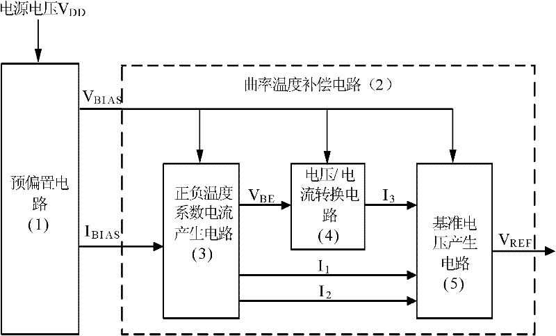
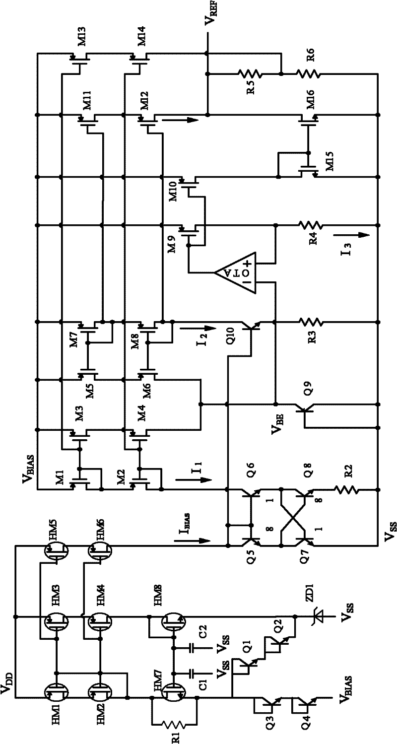
[0027] refer to figure 1 , The present invention includes a pre-bias circuit 1 and a curvature temperature compensation circuit 2 . Wherein: the curvature temperature compensation circuit 2 is mainly composed of a positive and negative temperature coefficient current generation circuit 3 , a voltage / current conversion circuit 4 and a reference voltage generation circuit 5 . The positive and negative temperature coefficient current generation circuit 3 includes a voltage input terminal, a current input terminal, and a voltage output terminal V BEand two current outputs I 1 , I 2 ; Voltage / current conversion circuit 4 includes two voltage input terminals and one current output terminal I 3 ; The reference voltage generation circuit 5 includes one voltage input terminal, three current input terminals and one voltage output terminal V REF . The voltage input ...


PUM


Abstract

The invention discloses a band-gap reference voltage source with wide input belt point curvature compensation, and the band-gap reference voltage source is mainly used for solving the problems of low source rejection ratio and low temperature stability. The band-gap reference voltage source comprises a pre-bias circuit (1), a positive and negative temperature coefficient current generation circuit (3), a voltage / current conversion circuit (4) and a reference voltage generation circuit (5). The output voltage VBIAS of the pre-bias circuit (1) is output to the positive and negative temperature coefficient current generation circuit (3), the voltage / current conversion circuit (4) and the reference voltage generation circuit (5) respectively; the current IBIAS generated by the pre-bias circuit (1) is output to the positive and negative temperature coefficient current generation circuit (3); currents I1 and I2 generated by the positive and negative temperature coefficient current generation circuit (3) are output to the reference voltage generation circuit (5); and simultaneously, the voltage VBE generated by the positive and negative temperature coefficient current generation circuit (3) is converted into a current I3 by the voltage / current conversion circuit (4) and is output to the reference voltage generation circuit (5); and the reference voltage generation circuit (5) outputsthe reference voltage VREF. The band-gap reference voltage source is high in rejection ratio and excellent in temperature stability and can be applied to an integrated circuit with wide input and high precision.

Description

technical field [0001] The invention belongs to the field of microelectronics and relates to a voltage reference circuit of an integrated circuit, in particular to a bandgap reference voltage source with wide input band curvature temperature compensation. Background technique [0002] The reference voltage source is an indispensable unit in many analog circuits and digital-analog hybrid integrated circuits. The normal operation and stable performance of the circuit system are inseparable from the stable reference voltage independent of temperature and power supply changes. With the increase of the complexity of the circuit system and the enhancement of the chip function, the requirements for some performance indicators of the reference voltage source are also increased. In some integrated circuit chips, it is often required to change the input power supply voltage range from a few volts to tens of volts, such as power MOSFETs that convert direct current to alternating curren...

Claims


Application Information

Patent Timeline
Patent Type & Authority Applications(China)
IPC IPC(8): G05F3/18
Inventor 来新泉叶强马行何惠森刘晨
Owner XIDIAN UNIV
Why Eureka
Try Eureka