
sonos structure, sonos memory

A technology of substrate and convex surface, applied in the field of SONOS structure and SONOS memory, can solve the problems of erasure saturation and electron incomplete tunneling, etc., and achieve the effect of erasing saturation

Inactive Publication Date: 2011-12-21
SHANGHAI HUAHONG GRACE SEMICON MFG CORP
View PDF6 Cites 4 Cited by
  • Summary
  • Abstract
  • Description
  • Claims
  • Application Information

AI Technical Summary

Problems solved by technology

The SONOS memory of the prior art described above has the problem of erase saturation, that is, the electrons in the trapped charge layer cannot completely tunnel out of the trapped charge layer

Method used


Image

  • sonos structure, sonos memory
  • sonos structure, sonos memory
  • sonos structure, sonos memory

Examples


Embodiment Construction

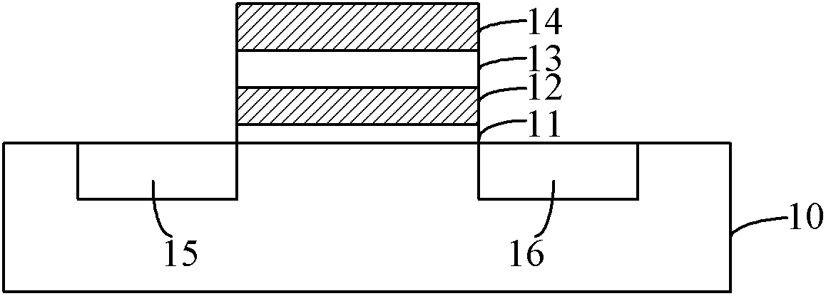
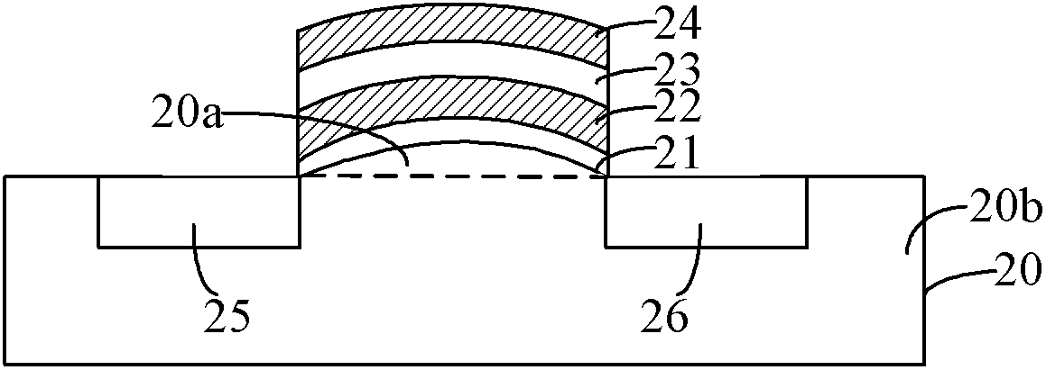
[0024] Based on the working principle of SONOS memory described above, SONOS memory uses FN tunneling effect (Fowler-Nordheim Tunneling) to erase: the strong field between the gate and the substrate makes the electrons in the trapped charge layer tunnel through the tunnel The tunneling dielectric layer enters the substrate. When the thickness of the tunneling dielectric layer is determined, the tunneling process is mainly determined by the electric field in the tunneling dielectric layer. The greater the electric field strength, the easier the tunneling occurs, that is, the trapping of the charge layer The easier it is for electrons to tunnel into the substrate. There are two tunneling processes in the SONOS structure: tunneling one, electrons tunnel from the gate through the top dielectric layer to the trapped charge layer, and tunneling two: electrons tunnel from the trapped charge layer through the tunneling dielectric layer to the substrate. In the traditional flat SONOS st...


PUM


Abstract

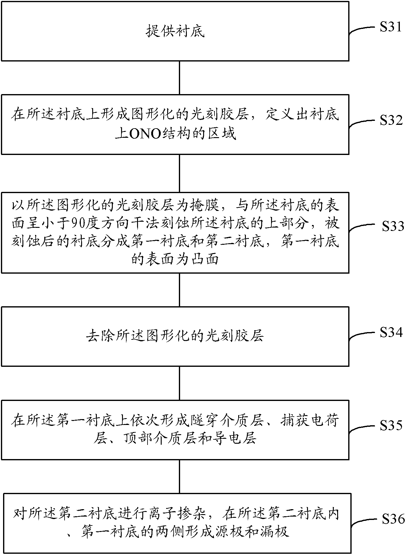
A SONOS structure and a SONOS memory, the SONOS structure includes: a substrate, the substrate includes a first substrate and a second substrate, the first substrate is located on the second substrate, the first A substrate defines the region of the ONO structure, and the surface of the first substrate is a convex surface; the tunneling dielectric layer, charge trapping layer, top dielectric layer and conductive layer located on the first substrate in sequence, the The upper and lower surfaces of the tunneling dielectric layer, the charge trapping layer, the top dielectric layer, and the conductive layer are all convex; the source and the drain are located in the second substrate and are respectively located in the first substrate. sides. The problem of erasing saturation of the SONOS memory in the prior art can be solved.

Description

Technical field [0001] The present invention relates to the field of semiconductor technology, in particular to SONOS structure and SONOS memory. Background technique [0002] Generally, semiconductor memory used to store data is divided into volatile memory and non-volatile memory. Volatile memory is prone to lose its data when power is interrupted, while non-volatile memory can save it even when power is interrupted. data. Compared with other non-volatile storage technologies (for example, disk drives), non-volatile semiconductor memory is relatively small. Therefore, non-volatile memory has been widely used in mobile communication systems, memory cards, and so on. [0003] The non-volatile memory cell can be realized by one of the two main technologies of a floating gate structure or a SONOS (Silicon-Oxide-Nitride-Oxide-Silicon, SONOS for short) structure. The relatively thick tunnel oxide layer (70-120 angstroms) of floating gate memory provides good charge retention perform...

Claims


Application Information

Patent Timeline
IPC IPC(8): H01L29/792H01L27/115
Inventor 吴小利
Owner SHANGHAI HUAHONG GRACE SEMICON MFG CORP
Learn More