Electrostatic absorption type micro-quality sensor
A mass sensor and electrostatic adsorption technology, applied in the field of precision sensors, can solve problems such as unfixable measurement errors and dispersion of measured objects, and achieve the effects of improving measurement repeatability and accuracy, stable performance, and improving effective stiffness
- Summary
- Abstract
- Description
- Claims
- Application Information
AI Technical Summary
Problems solved by technology
Method used
Image
Examples
Embodiment 1
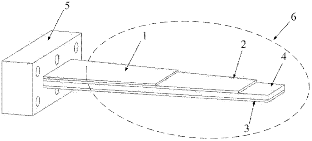
[0024] figure 1 A structural schematic diagram of an electrostatic adsorption micromass sensor is given, in which the multi-layer trapezoidal beam structure 6 is connected to the fixed block 5 to form a cantilever beam structure, and the upper insulating film 2 and the lower insulating film 3 are connected to the upper and lower surfaces of the conductive elastic plate 4 , by adjusting the length of the insulating film, different quality sensitive areas can be formed on the surface of the conductive elastic plate 4 . The piezoelectric film 1 is connected to the upper surface of the upper insulating film 2 to form electrical isolation with the conductive elastic plate 4, and the thickness of the upper insulating film 2 and the lower insulating film 3 is relatively large, so that the electrostatic adsorption force is smaller than the inertia of the measured object force. During the measurement process of the sensor, relying on the electrostatic adsorption of the conductive elas...
Embodiment 2
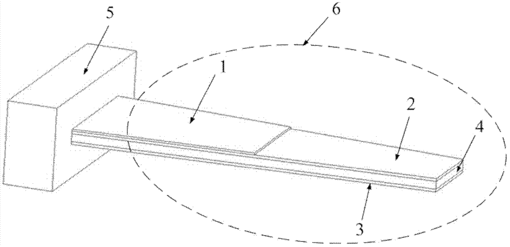
[0033] image 3A structural schematic diagram of another electrostatic adsorption micromass sensor is given. Aiming at the micromass measurement of tiny measured objects with conductive properties, on the basis of the first embodiment, the upper insulating film 2 is completely covered on the upper surface of the conductive elastic plate 4, and the lower insulating film 3 forms a fully enclosed electrostatic adsorption device. Wherein, the thickness of the lower insulating film 3 is three times that of the upper insulating film 2, so that the conductive measured object can be effectively adsorbed on the sensitive area of the trapezoidal cantilever beam.
Embodiment 3
[0035] Figure 4 A structural schematic diagram of another electrostatic adsorption micromass sensor is shown. On the basis of Embodiment 1, let the lower insulating film 3 and the upper insulating film 2 have the same size, and partially cover the conductive elastic plate 4, the upper and lower surfaces of the sensitive area of the conductive elastic plate 4 can absorb tiny measured objects, and the two layers of insulation The thickness of the film can make the electrostatic force generated by the conductive elastic plate 4 smaller than the inertial force of the tiny measured object. In addition, in this embodiment, the lower piezoelectric film 7 and the upper piezoelectric film 1 form a dual piezoelectric measurement to obtain higher sensitivity.
PUM
 Abstract
Description
Claims
Application Information


