Laser annealing platform device

A technology of laser annealing and wafer stage, used in electrical components, semiconductor/solid-state device manufacturing, circuits, etc., can solve problems such as inconvenient operation and complex structure, and achieve the effects of simple structure, reduced heat transfer flow, and reduced temperature

Active Publication Date: 2012-01-04
TSINGHUA UNIV
View PDF3 Cites 3 Cited by
  • Summary
  • Abstract
  • Description
  • Claims
  • Application Information

AI Technical Summary

Problems solved by technology

However, the existing loading and unloading auxiliary mechanism

Method used


Image

  • Laser annealing platform device
  • Laser annealing platform device
  • Laser annealing platform device

Examples


Embodiment Construction

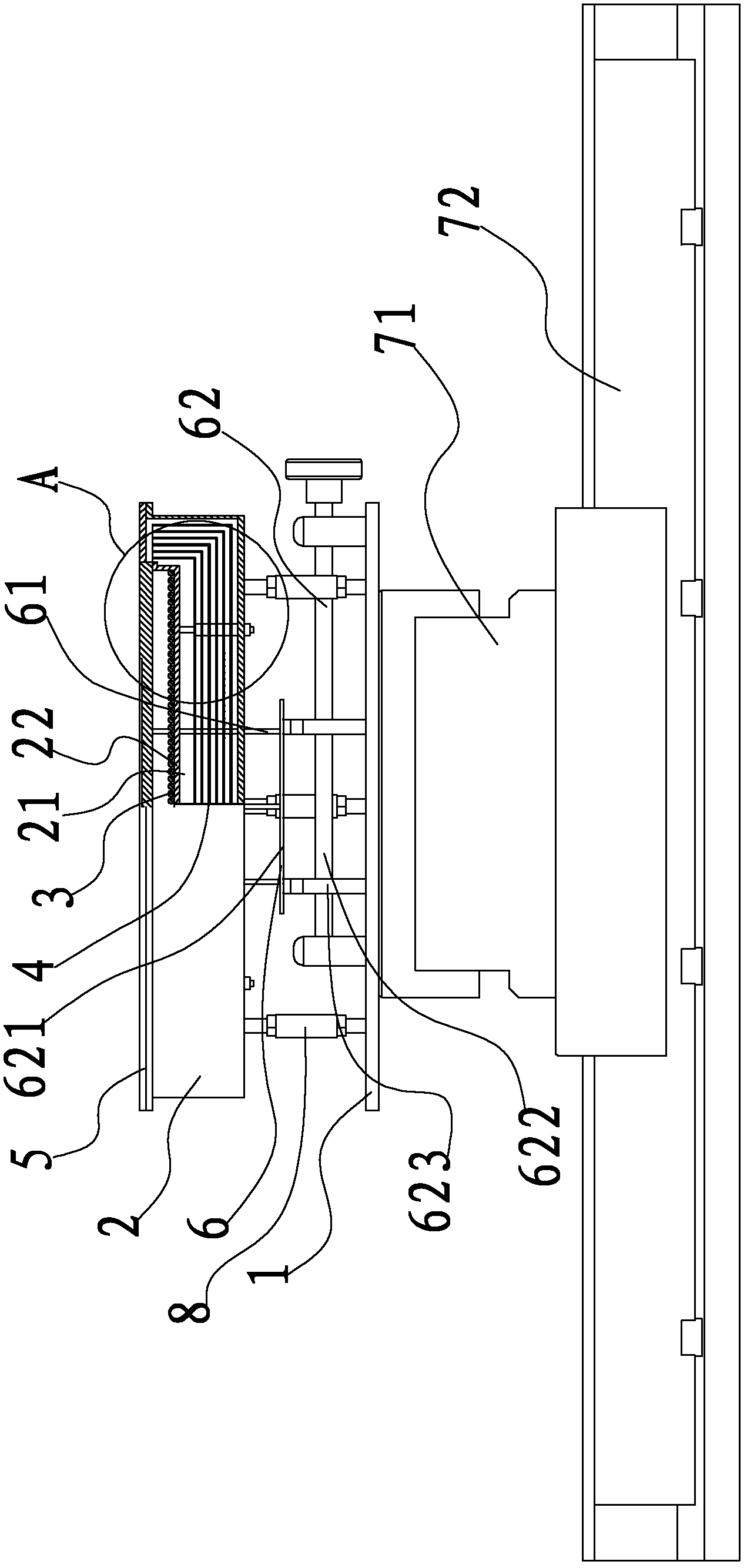
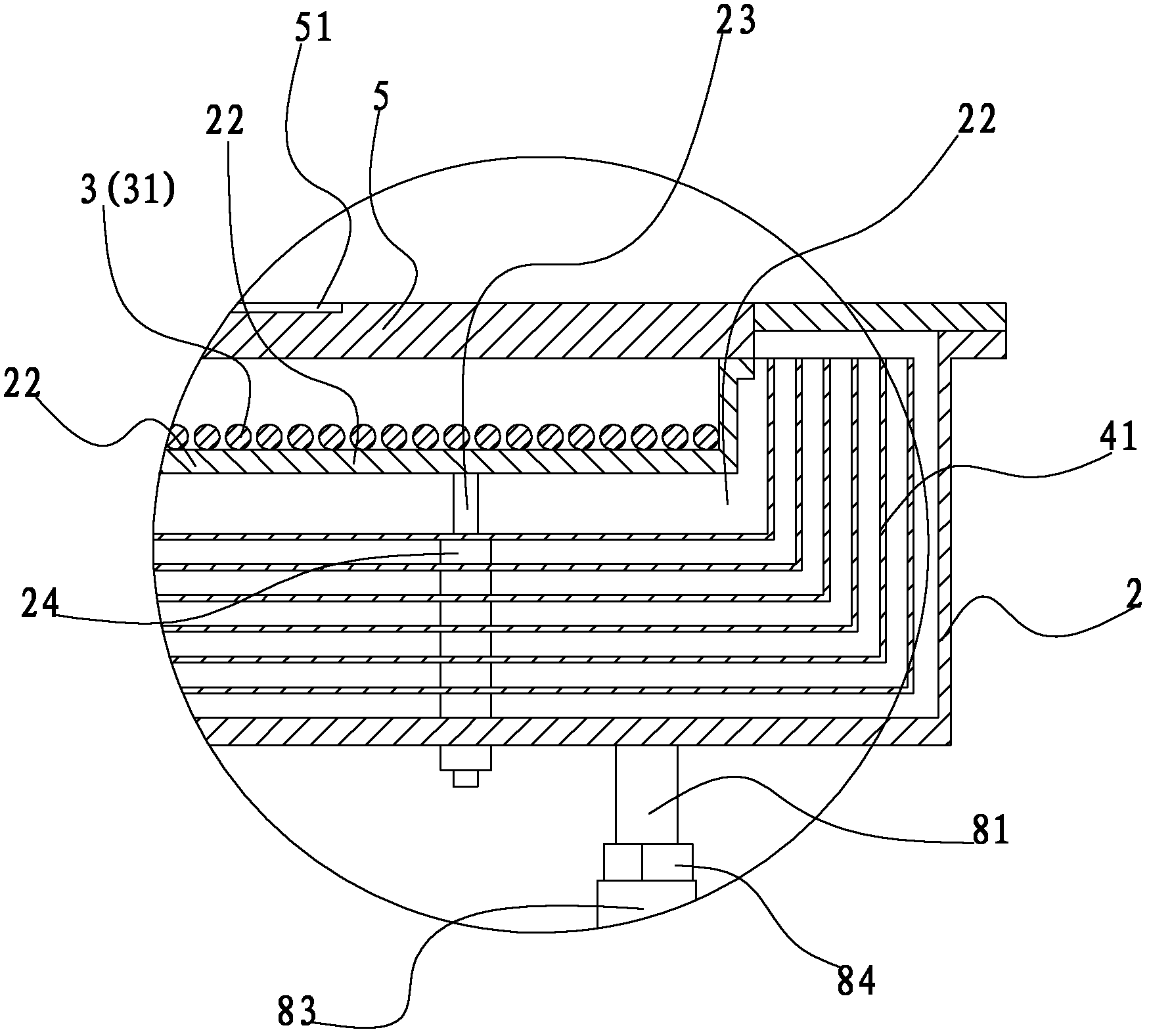
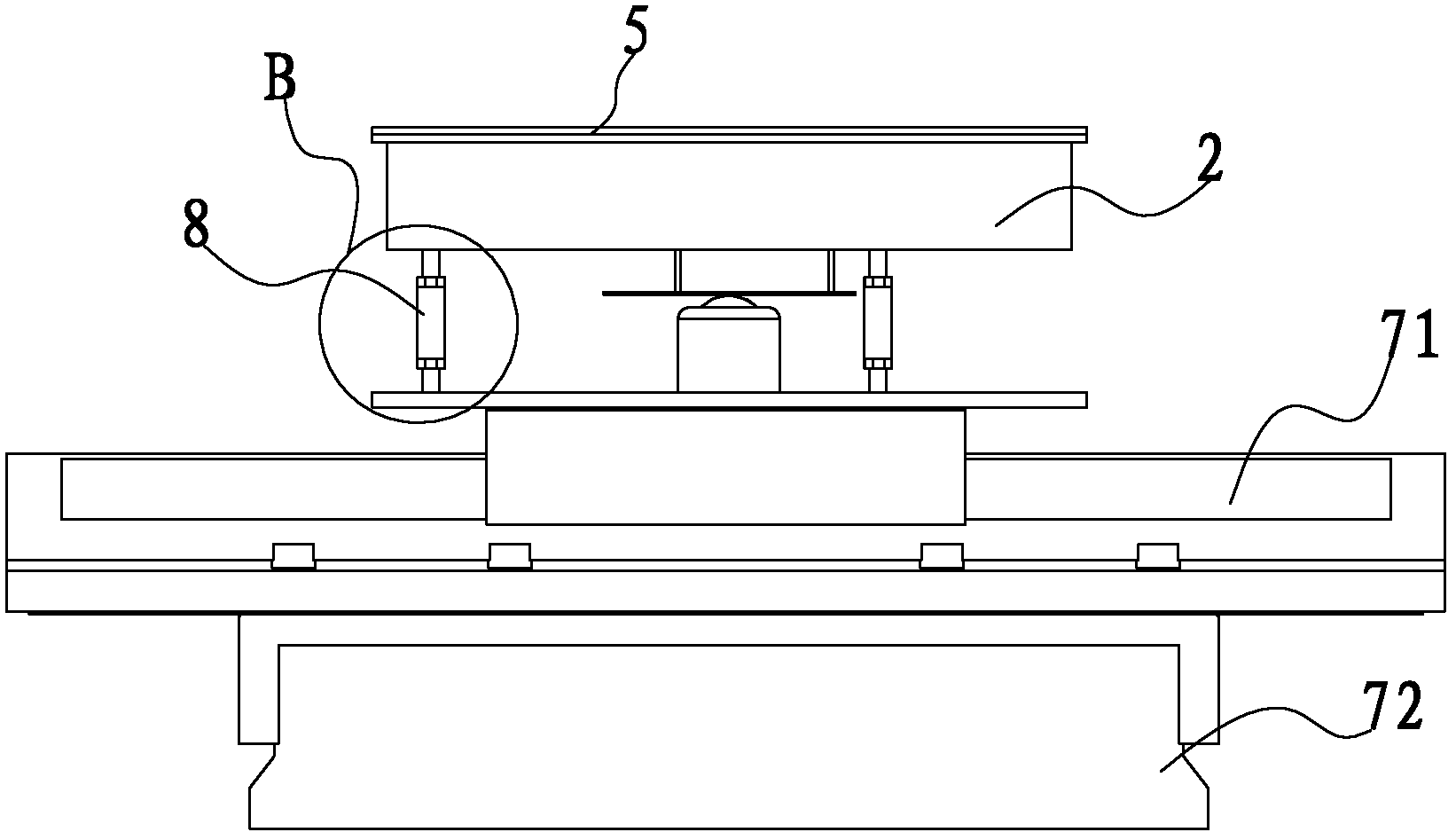
[0024] Embodiments of the present invention are described in detail below, examples of which are shown in the drawings, wherein the same or similar reference numerals designate the same or similar elements or elements having the same or similar functions throughout. The embodiments described below by referring to the figures are exemplary only for explaining the present invention and should not be construed as limiting the present invention.

[0025] In describing the present invention, it should be understood that the terms "center", "longitudinal", "transverse", "upper", "lower", "front", "rear", "left", "right", " The orientations or positional relationships indicated by "vertical", "horizontal", "top", "bottom", "inner", "outer", etc. are based on the orientation or positional relationships shown in the drawings, and are only for the convenience of describing the present invention and simplifying Describes, but does not indicate or imply that the device or element referred...


PUM


Abstract

The invention discloses a laser annealing platform device which comprises a base, a furnace casing, a heating assembly, a heat insulation assembly, a tray and a plate unloading assembly. A furnace chamber is limited in the furnace casing, the upper surface of the furnace chamber is open, and the furnace casing is supported on the base; the heating assembly is arranged in the furnace chamber; the heat insulation assembly is arranged between the heating assembly and the inner wall of the furnace casing; the tray is arranged on the top surface of the furnace casing and is provided with a throughhole which passes through the tray axially; the plate unloading assembly is arranged on the base and is positioned between the furnace casing and the base, and comprises a plurality of thimbles and adriving assembly, wherein the driving assembly is used for driving the plurality of thimbles to move along the upper and lower direction so that each thimble can pass through the corresponding through hole upward and extend upward to the upper surface of the tray. According to the laser annealing platform device provided by the invention, the structure is simple, and the heating for a silicon wafer is uniform; and when the silicon wafer is placed and unloaded, the plate unloading assembly plays a role of assistance, thus the silicon wafer is more convenient to place and unload.

Description

technical field [0001] The invention relates to the field of integrated circuit manufacturing, in particular to a silicon wafer laser annealing chip stage device used in integrated circuit manufacturing. Background technique [0002] Laser annealing is an important heat treatment link in the ultra-shallow junction fabrication process. When performing laser annealing on silicon wafers, it is necessary to achieve precise plane movement of the silicon wafer relative to the laser light source, and at the same time, in order to reduce the energy threshold, it is necessary to supplement the heating of the silicon wafer. The higher temperature heat source will affect the linear motor and precision guide rail of the lower motion platform, resulting in increased motion error. When loading and unloading the wafer, the silicon wafer is placed on the tray by vacuum tweezers and other tools, and then removed from the tray. At the same time, a loading and unloading auxiliary mechanism is...

Claims


Application Information

Patent Timeline
IPC IPC(8): H01L21/00H01L21/268
Inventor 张建富冯平法吴志军郁鼎文荣子光张云亮郑书友
Owner TSINGHUA UNIV
Why Eureka
Try Eureka