Testing device and testing method

一种测试设备、测试方法的技术,应用在测试船建造、测试介电强度、单个半导体器件测试等方向,能够解决设备变复杂、测试设备复杂等问题,达到减小负担的效果

Active Publication Date: 2012-01-11
FUJI ELECTRIC CO LTD
View PDF14 Cites 11 Cited by
  • Summary
  • Abstract
  • Description
  • Claims
  • Application Information

AI Technical Summary

Problems solved by technology

[0007] However, for the method of providing an insulating shield in the discharge path, a structure for placing the insulating shield at a predetermined position is required, which means that the test equipment may become complicated
[0008] Also for the method of testing in the state where the device under test is immersed in the insulating solution, handling the insulating solution means that the equipment used for the test may become complicated

Method used


Image

  • Testing device and testing method
  • Testing device and testing method
  • Testing device and testing method

Examples


no. 1 example

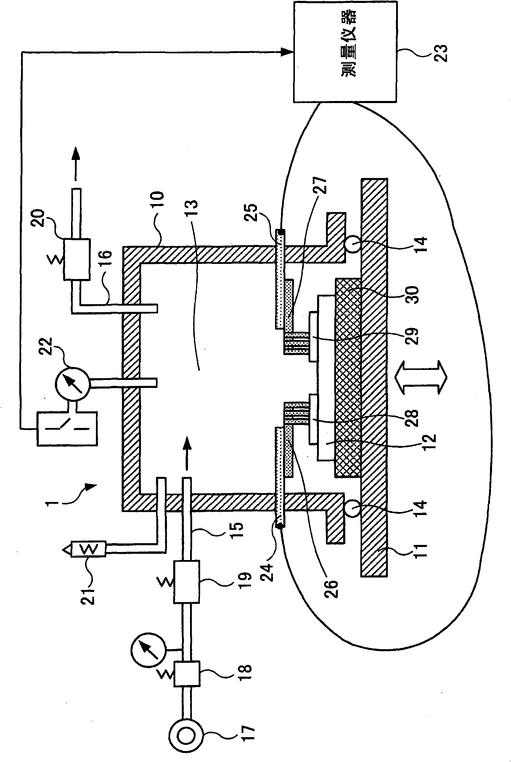
[0034] figure 1 is a diagram showing an example of the testing device according to the first embodiment.

[0035] The testing device 1 has a pressure vessel 10 , a bottom plate 11 , and a measuring instrument 23 . The pressure vessel 10 has an internal space 13 and can withstand a pressure to bring the internal space 13 to a predetermined pressure, and a device under test (DUT) 12 is tested in the internal space 13 . The pressure vessel 10 may also be referred to as, for example, a chamber. Here, it is assumed that the device under test 12 is a semiconductor device including the electrodes 28 and 29 as an example. The device under test 12 may also be any one of a semiconductor wafer, a semiconductor chip, a semiconductor package, or a semiconductor module. The test apparatus 1 may also be configured to appropriately use a configuration of a wafer detector, a processor, and the like according to the apparatus under test 12 as needed.

[0036] The bottom plate 11 is provided...

no. 2 example

[0079] Figure 4 is a diagram showing an example of a test device according to the second embodiment.

[0080] The difference between the test device 2 and the test device 1 lies in the shape of the pressure vessel, and a piston 31 and a servo motor 32 are additionally provided. In addition, although a safety valve is not provided, a safety valve may be provided. Other configurations are the same as those of the test device 1 .

[0081] The pressure vessel 33 has an opening at its top. The piston 31 is arranged to block the opening of the pressure vessel 33 . A servo motor 32 is provided on the piston 31 . The piston 31 raises or lowers the inner space 34 of the pressure vessel 33 under the control of the servo motor 32 .

[0082] At this time, the piston 31 moves along the inner wall 35 of the pressure vessel 33 while being in close contact with the inner wall 35 of the pressure vessel 33 . That is, the pressure vessel 33 functions as an air cylinder. The control of th...

no. 3 example

[0123] Figure 7 A and Figure 7 B is a diagram showing an example of a dielectric strength test according to the third embodiment. Figure 7 A is a top view of the device under test 40, and Figure 7 B is a cross-sectional view of the device under test 40 to which test electrodes 47a and 47b are attached.

[0124] Such as Figure 7 As shown in A, the device under test 40 has a frame electrode 41 , a plurality of lead terminals 42 and 43 , and a semiconductor chip 44 . A semiconductor chip 44 is formed on the frame electrode 41 , and the semiconductor chip 44 is electrically connected to the lead terminals 42 and 43 through an internal wire 45 . Furthermore, the frame electrode 41 , the plurality of lead terminals 42 and 43 , the semiconductor chip 44 , and the internal wire 45 are sealed with a resin 46 . Here, an end portion of the frame electrode 41 and an end portion of each of the lead terminals 42 and 43 are exposed from the resin 46 .

[0125] When testing, clamp ...


PUM


Abstract

The present invention provides a testing device and a testing method, used for realizing high voltage testing and reducing burden to the global environment, without causing complixity of a testing device or a device for testing.The testing device includes a pressure vessel, a mounting stand disposed in an internal space of the pressure vessel, on which a device to be tested is mounted, test electrodes, disposed in the internal space of the pressure vessel, that supply a test voltage to the device to be tested mounted on the mounting stand, and a pressurization unit that raises the pressure of the internal space of the pressure vessel. The test voltage is supplied from the test electrodes to the device to be tested mounted on the mounting stand, and testing of the device to be tested is carried out, in a condition that the pressure of the internal space of the pressure vessel is raised by the pressurization unit.

Description

technical field [0001] The invention relates to a testing device and a testing method for high-voltage testing of a tested device. Background technique [0002] There is a testing method by which a high test voltage is applied to a device under test and a high voltage test is performed on the device under test. Using this type of test method, dielectric breakdown will occur between the electrodes of the device under test, between the electrodes of the device under test and the test device, and cause discharge, which may cause damage to the device under test or the test device, and May cause the test of the device under test to not be performed correctly. [0003] Therefore, there is a way to place the tested equipment in a gas environment with high insulation, such as sulfur hexafluoride gas (SF 6 ), and the technology of high-voltage testing under the condition of ensuring the medium strength of the test environment. [0004] However, gases with high insulating propertie...

Claims


Application Information

Patent Timeline
Patent Type & Authority Applications(China)
IPC IPC(8): G01R31/26
CPCG01R31/129G01R31/2881G01R31/16
Inventor 吉田敦户谷浩之西泽徹内山诚三
Owner FUJI ELECTRIC CO LTD
Why Eureka
Try Eureka