Display device and method for manufacturing same

A technology for display devices and display pixels, which is applied to identification devices, organic semiconductor devices, instruments, etc., can solve problems such as increased defective rate of short-circuited pixels, achieve the effect of improving display quality and ensuring the function of capacitance retention

Inactive Publication Date: 2014-11-26
JOLED INC
View PDF6 Cites 0 Cited by
  • Summary
  • Abstract
  • Description
  • Claims
  • Application Information

AI Technical Summary

Problems solved by technology

Therefore, this storage capacitor element is easily affected by particles and the like present between the electrodes, and it becomes a factor that increases the pixel defect rate due to short-circuit failure.

Method used


Image

  • Display device and method for manufacturing same
  • Display device and method for manufacturing same
  • Display device and method for manufacturing same

Examples


Embodiment approach 1

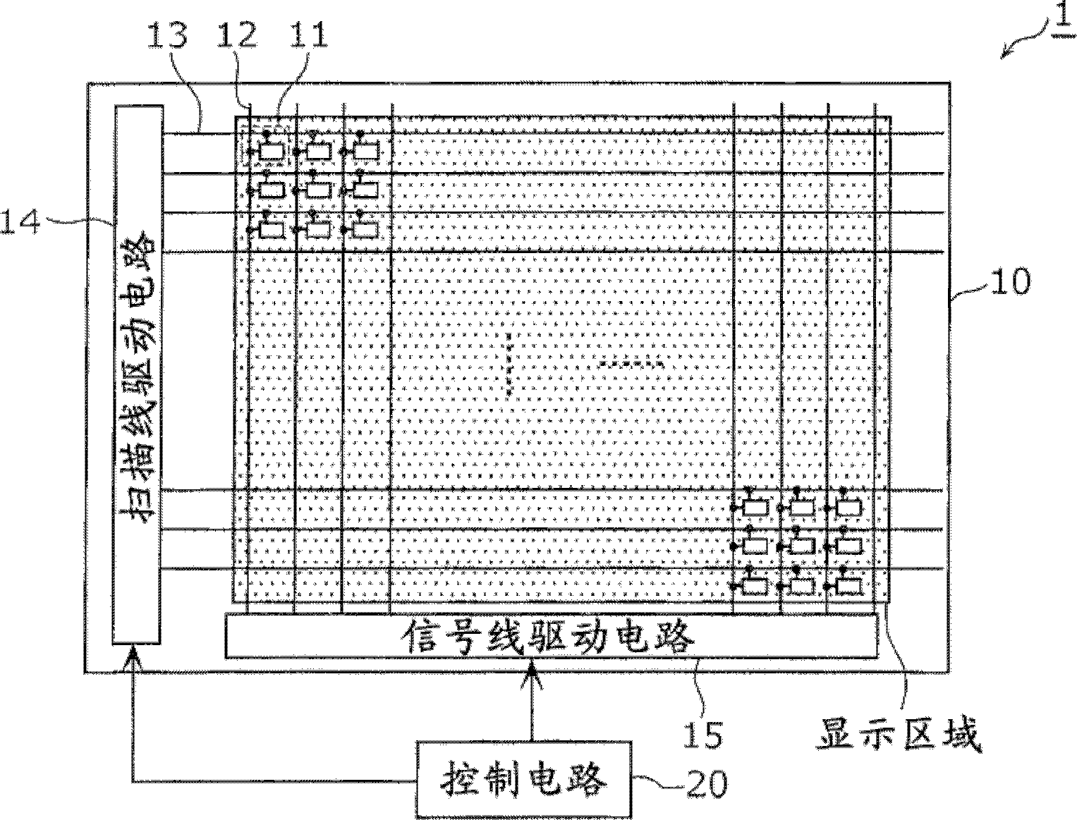
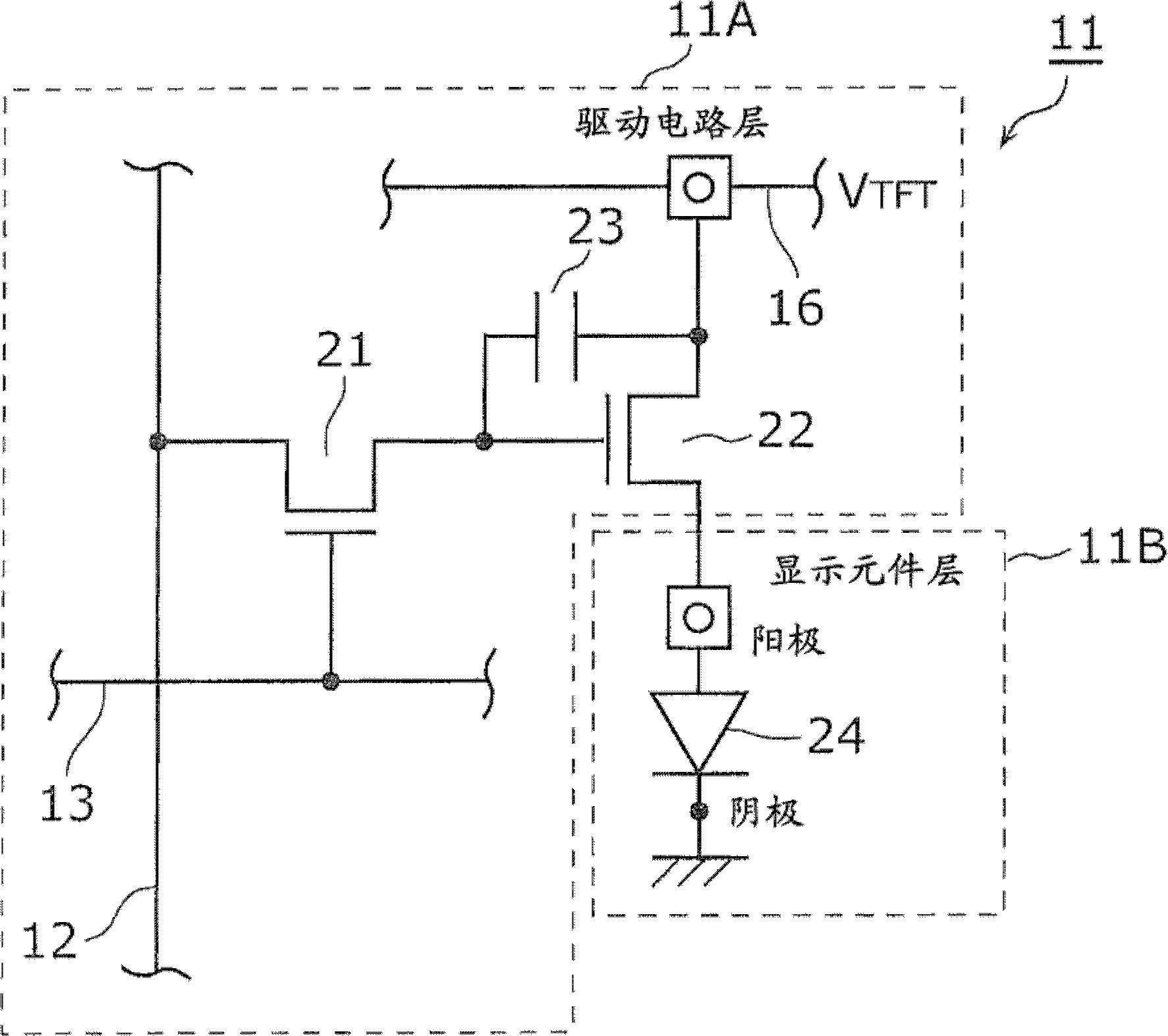
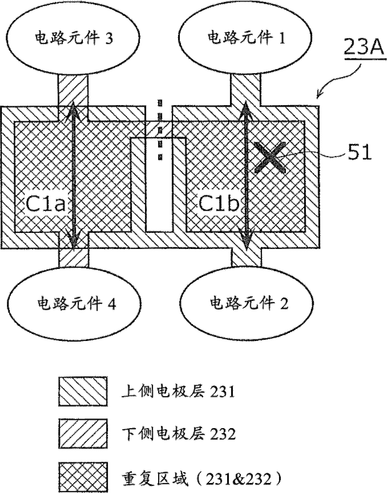
[0089] In the display device of this embodiment, a plurality of display pixels are arranged two-dimensionally, and a display element layer and a driving circuit layer for driving the display element layer are stacked in the plurality of display pixels. The drive circuit layer includes a parallel-plate capacitive element having an upper electrode layer and a lower electrode layer arranged to face each other in the stacking direction. The upper electrode layer includes: a first upper capacitor electrode portion having a circuit wiring function for connecting the first circuit element and the second circuit element; connected to the second upper capacitor electrode portion. The lower electrode layer includes: a first lower capacitive electrode portion having a circuit wiring function for connecting the third circuit element and the fourth circuit element; connected to the second lower capacitor electrode portion. The capacitive element is between the first upper capacitive elec...

Embodiment approach 2

[0159] In this embodiment mode, a method for manufacturing the display device of the present invention will be described. The method of manufacturing a display device of the present invention includes a step of forming a driving circuit layer, a step of forming a display element layer, a step of inspecting a pixel circuit, and a step of repairing a storage capacitor element. Here, the description will focus on steps different from those in the conventional display device manufacturing method, namely, the formation step of the storage capacitor element 23A included in the drive circuit layer, and the inspection step and repair step of the pixel circuit.

[0160] Figure 8 It is a flowchart showing the manufacturing method of the display device according to Embodiment 2 of the present invention.

[0161] First, the drive circuit layer 11A in which the storage capacitor element 23A and the switching transistor 21 as its peripheral elements, the drive transistor 22 , circuit wiri...

Embodiment approach 3

[0175] In this embodiment, the layout configuration and effects of light-emitting pixels in which the storage capacitor element of Embodiment 1 and other circuit elements constituting the driving circuit layer 11A are arranged will be described.

[0176] Figure 9A It is a first layout diagram of light-emitting pixels included in a conventional display device. The layout shown in this figure is the layout of one light-emitting pixel, and the signal line 12, the scanning line 13, the switching transistor 21, the driving transistor 22, the storage capacitance element having the electrostatic capacitance C1, and the circuit wiring are drawn. In addition, the switching transistor 21 and the driving transistor 22 are bottom gate type, the layer where the gate electrode is formed is the lower electrode layer, and the layer where the source electrode and the drain electrode are formed is the upper electrode layer. Although the area ratio of the light-emitting pixel is high, the stor...


PUM


Abstract

The display device includes stacked layers including a display element layer and a control layer including a capacitor including an upper electrode layer and a lower electrode layer that face each other in a layer-stacking direction, wherein the upper electrode layer includes a first upper capacitor electrode connecting two circuit elements, a disconnectable portion, and a second upper capacitor electrode connected to the first upper electrode layer through the disconnectable portion, and the lower electrode layer includes a first lower capacitor electrode connecting two circuit elements, a disconnectable portion, and a second lower capacitor electrode connected to the first lower electrode layer through the disconnectable portion. The capacitor has a capacitance each between the first upper capacitor electrode and the second lower capacitor electrode, and the first lower capacitor electrode and the second upper capacitor electrode.

Description

technical field [0001] The present invention relates to a display device and a manufacturing method thereof, in particular to a display device with a modifiable pixel structure and a manufacturing method thereof. Background technique [0002] An organic EL display using an organic electroluminescent element (hereinafter, referred to as an organic EL element) is known as an image display device using a current-driven light-emitting element. Since this organic EL display has advantages of excellent viewing angle characteristics and low power consumption, it is attracting attention as a candidate for a next-generation FPD (Flat Panel Display, flat panel display). [0003] Generally, organic EL elements constituting a pixel are arranged in a matrix. For example, in an active matrix organic EL display, a thin film transistor (TFT: Thin Film Transistor) is provided at the intersection of a plurality of scanning lines and a plurality of data lines, and a storage capacitance elemen...

Claims


Application Information

Patent Timeline
Patent Type & Authority Patents(China)
IPC IPC(8): G09F9/30G09F9/00H01L27/32
CPCH01L27/3265H01L2251/568H01L27/1255Y10T29/49002H10K59/1216H10K71/861G09F9/00G09F9/30
Inventor 白水博田鹿健一
Owner JOLED INC
Why Eureka
Try Eureka