Method for manufacturing semiconductor device
A manufacturing method and semiconductor technology, applied in the direction of semiconductor/solid-state device manufacturing, electrical components, circuits, etc., to achieve the effect of reducing height, expanding the photolithography process window, and eliminating coupling capacitance
- Summary
- Abstract
- Description
- Claims
- Application Information
AI Technical Summary
Problems solved by technology
Method used
Image
Examples
Embodiment 1
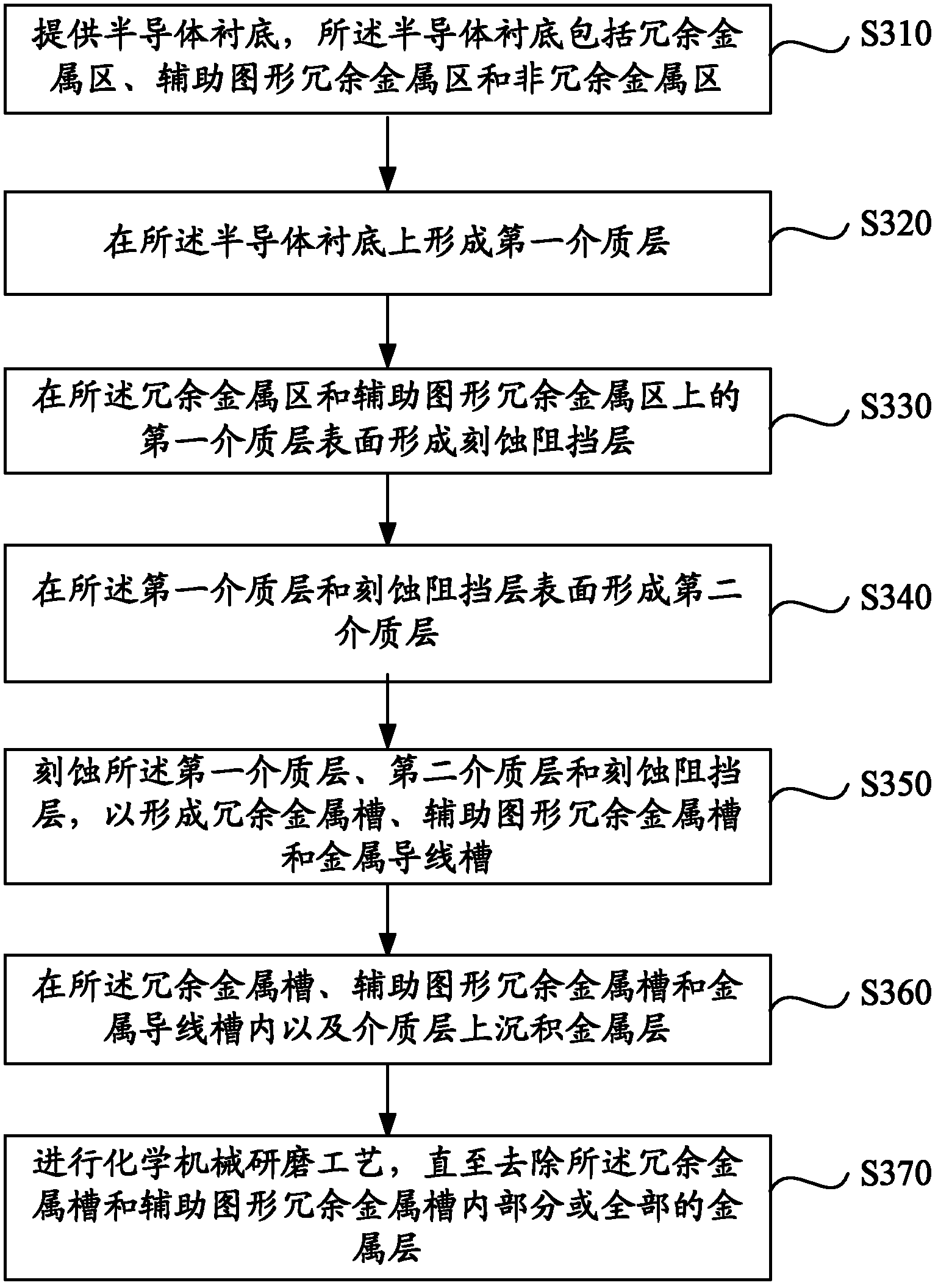
[0020] Please refer to image 3 , which is a schematic flow chart of the manufacturing method of the semiconductor device of the present invention. Such as image 3 As shown, the manufacturing method of the semiconductor device includes the following steps:
[0021] Step S310: providing a semiconductor substrate, the semiconductor substrate including a redundant metal area, an auxiliary pattern redundant metal area and a non-redundant metal area;
[0022] Step S320: forming a first dielectric layer on the semiconductor substrate;
[0023] Step S330: forming an etching barrier layer on the surface of the first dielectric layer on the redundant metal area and the auxiliary pattern redundant metal area;
[0024] Step S340: forming a second dielectric layer on the surface of the first dielectric layer and the etch stop layer;
[0025] Step S350: Etching the first dielectric layer, the second dielectric layer and the etch barrier layer to form redundant metal grooves, auxiliary...
Embodiment 2
[0038] Such as Figure 5A As shown, firstly, a semiconductor substrate 500 is provided, and the semiconductor substrate 500 includes a redundant metal region 502, an auxiliary pattern redundant metal region 503 and a non-redundant metal region 501, the redundant metal region 502, the auxiliary pattern redundant The region of the semiconductor substrate outside the metal region 503 is the non-redundant metal region 501 . Subsequently, a first dielectric layer 511 is formed on the semiconductor substrate 500 .
[0039] refer to Figure 5B , and then, forming an etch barrier layer on the surface of the first dielectric layer 511, and removing the etch barrier layer on the non-redundant metal region 501 by using photolithography and etching processes, so that the redundant metal region 502. Form an etching barrier layer 530 on the surface of the first dielectric layer on the auxiliary pattern redundant metal region 503, and the etching rate of the etching barrier layer 530 is lo...
Embodiment 3
[0047] Such as Figure 6A As shown, first, a semiconductor substrate 600 is provided, and the semiconductor substrate 600 includes a redundant metal region 602, an auxiliary pattern redundant metal region 603 and a non-redundant metal region 601, the redundant metal region 602, the auxiliary pattern redundant The region of the semiconductor substrate outside the metal region 603 is the non-redundant metal region 601 . Subsequently, a first dielectric layer 611 is formed on the semiconductor substrate 600 .
[0048] refer to Figure 6B , and then, forming an etch barrier layer on the surface of the first dielectric layer 611, and removing the etch barrier layer on the non-redundant metal region 601 by photolithography and etching processes, so that the redundant metal region 602. Form an etching barrier layer 630 on the surface of the first dielectric layer on the auxiliary pattern redundant metal region 603, and the etching rate of the etching barrier layer 630 is lower than...
PUM
 Abstract
Description
Claims
Application Information


