
Thermal system and technology for producing float zone doped single crystal silicon having size phi of 6 inches

A silicon single crystal, thermal system technology, applied in the direction of single crystal growth, single crystal growth, self-area melting method, etc., can solve the problem of increasing the risk of bud breaking, and achieve the effect of meeting the needs

Active Publication Date: 2012-02-22
ZHONGHUAN ADVANCED SEMICON MATERIALS CO LTD +1
View PDF6 Cites 20 Cited by
  • Summary
  • Abstract
  • Description
  • Claims
  • Application Information

AI Technical Summary

Problems solved by technology

Doping the single crystal is to introduce impurity atoms into the single crystal lattice, which increases the risk of broken buds

Method used


Image

  • Thermal system and technology for producing float zone doped single crystal silicon having size phi of 6 inches
  • Thermal system and technology for producing float zone doped single crystal silicon having size phi of 6 inches

Examples


Embodiment Construction

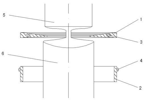
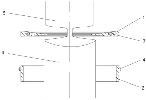
[0019] The present invention will be further described below in conjunction with embodiment and accompanying drawing. refer to figure 1 , a thermal system for producing molten gas-doped silicon single crystals in a Φ6-inch area includes a coil 1 and an insulating cylinder 2. The upper surface of the coil 1 is an inclined multi-step coil. The outer diameter of the coil 1 is Φ300mm, the inner diameter is Φ50mm, and the thickness is 30mm. The heat preservation tube 2 has a diameter of Φ300mm and a height of 100mm. The distance between the coil 1 and the insulation cylinder 2 is 100mm. The cooling water channel 3 of the coil 1 and the cooling water channel 4 of the insulation cylinder 2 are respectively located inside the two.

[0020] The equipment used to produce Φ6-inch molten gas-doped silicon single crystal is PVA FZ-30 type, and the specific steps of the process are as follows:

[0021] 1. First open the furnace door, wipe the inner wall of the furnace door, the upper fur...


PUM

PropertyMeasurementUnit
thicknessaaaaaaaaaa
diameteraaaaaaaaaa
heightaaaaaaaaaa

Abstract

The invention relates to a thermal system and a technology for producing a float zone doped single crystal silicon having a size phi of 6 inches. The thermal system comprises a coil and a heat preservation cylinder. An upper surface of the coil has an inclined multi-stepped coil structure. An external diameter phi of the coil is in a range of 350+50 / -50 millimeters. An internal diameter phi of the coil is in a range of 50+2 / -2 millimeters. The thickness of the coil is in a range of 30+2 / -2 millimeters. A diameter phi of the heat preservation cylinder is in a range of 350+50 / -50 millimeters. The height of the heat preservation cylinder is in a range of 100+20 / -20 millimeters. A distance between the coil and the heat preservation cylinder is in a range of 100+50 / -50 millimeters. The technology is characterized in that impurity gas is fed into a furnace chamber in shoulder extension, wherein a lower shaft rotating speed is in a range of 7 to 10 revolutions per minute and a shoulder extension angle is in a range of 40+2 / -2 degrees; and in equal-diameter growth, a lower shaft has a falling speed of 3 to 4 millimeters per minute and a rotating speed of 3 to 5 revolutions per minute and coil pulser power is 60 to 70% of rated power. Through the thermal system which is a novel thermal system and adjustment on technological parameters, the float zone doped single crystal silicon having a size phi of 6 inches can be successfully prepared by drawing, and dislocation and burr generation problems produced easily in production of a float zone doped single crystal silicon with a large size are solved, and thus market demands on single crystal silicon with a large size are satisfied.

Description

technical field [0001] The invention relates to a method for producing silicon single crystals, in particular to a thermal system and process for producing silicon single crystals doped with molten gas in a Φ6-inch zone. Background technique [0002] In order to increase productivity, reduce costs, and increase profits, semiconductor device manufacturers are gradually requesting to increase the diameter of silicon wafers. Larger diameters are an eternal topic for the semiconductor device industry and the material industry. However, in the production process of zone melting silicon single crystal, with the increase of single crystal diameter, its crystal formation becomes more and more difficult. [0003] For single crystals with a melting diameter in the drawing area, since the center of the single crystal dissipates heat slowly and the edges dissipate heat quickly, the solid-liquid interface of the single crystal is in the shape of a concave bowl. The edge of the single cr...

Claims


Application Information

Patent Timeline
Patent Type & Authority Applications(China)
IPC IPC(8): C30B13/20C30B29/06
Inventor 高树良张雪囡王彦君靳立辉康冬辉王遵义李建弘沈浩平
Owner ZHONGHUAN ADVANCED SEMICON MATERIALS CO LTD
Learn More