Printed circuit board and power supply module

A printed circuit board, electromagnetic technology, applied in the field of electronics, can solve the problems of reducing the cross-sectional area of ​​the conductor, high impedance of the switching converter, unable to meet the high power density of the power module, etc., reducing the AC impedance and increasing the conduction cutoff. Area, the effect of reducing the skin effect

Active Publication Date: 2013-10-02
HUAWEI TECH CO LTD
View PDF4 Cites 0 Cited by
  • Summary
  • Abstract
  • Description
  • Claims
  • Application Information

AI Technical Summary

Problems solved by technology

However, the PCB in the switching converter of the existing power module is mainly composed of a planar conductive layer. When the switching frequency in the switching converter is increased, the skin effect of the planar conductive winding in the planar conductive layer of the PCB is more obvious, that is At high switching frequency, the current in the plane conductive layer of the PCB tends to the surface of the conductor, the penetration depth of the current in the plane conductive layer becomes smaller, and the cross-sectional area of ​​the conductor that actually conducts current in the same plane conductive layer is relatively reduced, by This leads to high impedance of the switching converter at high switching frequency, which cannot meet the high power density requirements of the power module

Method used


Image

  • Printed circuit board and power supply module
  • Printed circuit board and power supply module
  • Printed circuit board and power supply module

Examples


Embodiment Construction

[0020] In order to make the purpose, technical solutions and advantages of the embodiments of the present invention clearer, the technical solutions in the embodiments of the present invention will be clearly and completely described below in conjunction with the drawings in the embodiments of the present invention. Obviously, the described embodiments It is a part of embodiments of the present invention, but not all embodiments. Based on the embodiments of the present invention, all other embodiments obtained by persons of ordinary skill in the art without creative efforts fall within the protection scope of the present invention.

[0021] The term "and / or" in this article is just an association relationship describing associated objects, which means that there can be three relationships, for example, A and / or B can mean: A exists alone, A and B exist simultaneously, and there exists alone B these three situations. In addition, the character " / " in this article generally ind...


PUM


Abstract

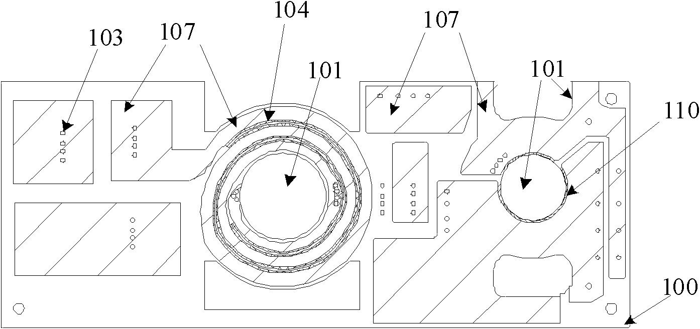
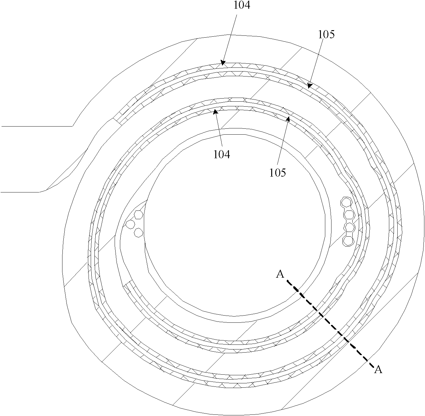
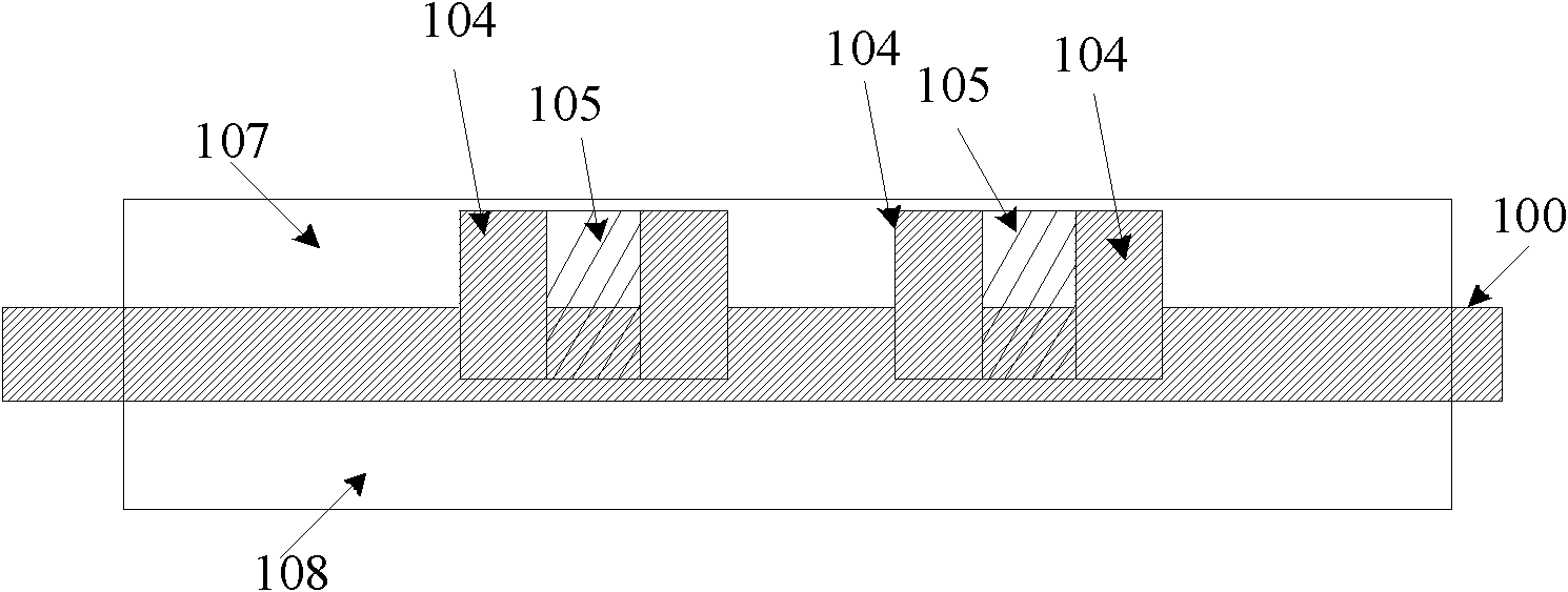
Embodiments of the present invention provide a printed circuit board and a power module. The printed circuit board comprises an insulating layer, a first planar conductive layer located above the insulating layer, and a second planar conductive layer located below the insulating layer. The insulating layer, the first planar conductive layer and the second planar conductive layer each are provided with a magnetic core groove having a penetrating magnetic core. The printed circuit board further comprises: at least one group of vertical conductive winding, configured to cooperate with the magnetic core mounted in the magnetic core groove to perform electromagnetic conversion. In the direction perpendicular to the insulating layer, one side of the at least one group of vertical conductive winding is located a position on the insulating layer or the first planar conductive layer except the magnetic core groove, and the other side of the at least one group of vertical conductive winding is located on a position on the insulating layer or the second planar conductive layer except the magnetic core groove. The printed circuit board can expand the sectional area of the conductive winding, and reduce the alternating current impedance of the power module.

Description

technical field [0001] Embodiments of the present invention relate to electronic technology, and in particular to a printed circuit board and a power supply module. Background technique [0002] Currently, a switching converter may be generally called a power module. In an existing power module, the primary winding and the secondary winding of a transformer may be composed of multiple planar conductive layers in a printed circuit board (PCB for short). [0003] In actual application scenarios, increasing the power density of the power module while reducing the volume of the power module has become a current demand. However, the PCB in the switching converter of the existing power module is mainly composed of a planar conductive layer. When the switching frequency in the switching converter is increased, the skin effect of the planar conductive winding in the planar conductive layer of the PCB is more obvious, that is At high switching frequency, the current in the plane con...

Claims


Application Information

Patent Timeline
Patent Type & Authority Patents(China)
IPC IPC(8): H05K1/18H02M1/00
CPCH05K2201/09672H05K2201/086H05K1/165H05K1/029H01F27/2804H01F2027/2819
Inventor 侯召政毛恒春傅电波黄良荣
Owner HUAWEI TECH CO LTD
Why Eureka
Try Eureka