
Device and method for removing electronic devices/components and soldered tin from waste circuit boards

A technology for electronic components and waste circuit boards, applied in auxiliary devices, welding equipment, metal processing and other directions, can solve the problems of volatilization of toxic elements, high energy consumption, and low heat utilization rate in circuit boards, and reduce labor intensity. , The effect of ensuring air quality and accelerating air circulation

Inactive Publication Date: 2012-03-14
苏州伟翔电子废弃物处理技术有限公司
View PDF6 Cites 12 Cited by
  • Summary
  • Abstract
  • Description
  • Claims
  • Application Information

AI Technical Summary

Problems solved by technology

[0006] Through research and comparison, it is found that the automatic or semi-automatic component removal equipment used in foreign countries is generally expensive and not suitable for my country's national conditions; the domestic use of hot air desoldering technology, although the components can be disassembled, due to high energy consumption, the heat utilization rate is low , and heating in the air will volatilize or oxidize the toxic elements in the circuit board
Due to the low heat transfer coefficient of air, the temperature must be increased to make the solder reach the melting temperature, which will easily cause overheating damage to components and reduce the recovery rate of components

Method used


Image

  • Device and method for removing electronic devices/components and soldered tin from waste circuit boards
  • Device and method for removing electronic devices/components and soldered tin from waste circuit boards

Examples


Embodiment Construction

[0021] The present invention will be further described below in conjunction with the accompanying drawings.

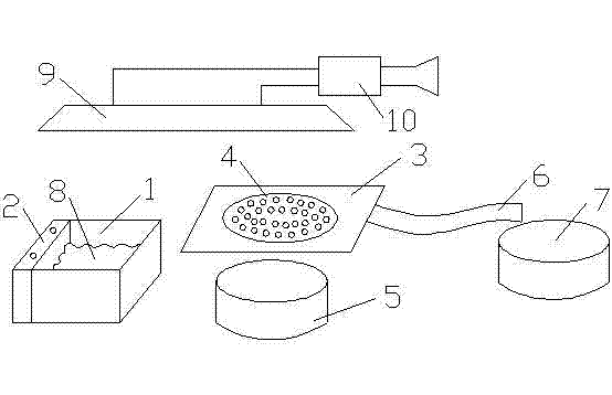
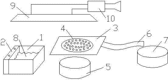
[0022] Such as figure 1 As shown, a device for removing electronic components and solder of waste circuit boards includes a component collection box 5, a circuit board collection box 7 and a vibrating component removal platform 3, and also includes a tin melting furnace 1. The tin melting furnace 1 includes a temperature control platform 2, and solder 8 is placed in the tin melting furnace 1. An air extraction device 9 and a gas adsorption purification device 10 connected to the air extraction device 9 are installed above the tin melting furnace 1 and the component removal platform 3 . A screen 4 is arranged on the component removal platform 3 , the component collection box 5 is located below the screen 4 , and a conveyor belt 6 is installed between the component removal platform 3 and the circuit board collector 7 .

[0023] The method for removing electronic compon...


PUM


Abstract

The invention discloses a device for removing electronic devices / components and soldered tin from waste circuit boards, which comprises a devices / components collecting box, a circuit board collecting box and a devices / components dismantling platform. The device further comprises a tin-melting furnace, wherein soldering tin is placed in the tin-melting furnace. The invention further discloses a method for removing the electronic devices / components and the soldered tin from the waste circuit boards by using the device. With the adoption of the device and the method for removing the electronic devices / components and the soldered tin from the waste circuit boards, the problems that the energy consumption is large, the heat utilization is low, and harmful elements in the circuit boards can volatilize or be oxidized when the electronic devices / components and the soldered tin are removed in the prior art are solved; through using molten soldering tin in the tin-melting furnace for heat transfer, the efficiency is increased, the energy consumption is lowered, and the manually operating intensity is lowered; meanwhile, peculiar smells and harmful gases and the like generated in a processing process are subjected to an adsorption treatment by using a negative-pressure absorption manner, and then, are discharged outdoors, the air circulation is accelerated, and the air quality of an operating environment is ensured.

Description

technical field [0001] The invention relates to a device and method for removing electronic components and solder of waste circuit boards, and belongs to the technical field of environmental protection. Background technique [0002] With the acceleration of social progress and technological development, the penetration rate of electronic and electrical products is getting higher and higher, and the speed of replacement is also getting faster and faster, resulting in a large number of electronic and electrical products being discarded. Printed circuit boards are widely used in electronic and electrical products, so the amount of scrapped printed circuit boards is also very large. [0003] Since printed circuit boards contain a variety of heavy metals, if they are discarded in nature, they will pollute soil and groundwater, causing irreparable economic and environmental losses. In addition, printed circuit boards also contain a variety of compounds, which will produce a large...

Claims


Application Information

Patent Timeline
Patent Type & Authority Applications(China)
IPC IPC(8): B23K3/00B23K3/08B23K1/018
Inventor 康俊峰李春航朱孝东
Owner 苏州伟翔电子废弃物处理技术有限公司
Learn More