Method for forming metal compound film

A metal compound and thin film technology, applied in the direction of metal material coating process, ion implantation plating, coating, etc., can solve the problems of reduced adhesion of titanium film, increased cost, reduced reliability of semiconductor devices, etc., to avoid changes. Effect

Inactive Publication Date: 2012-03-21
SEMICON MFG INT (SHANGHAI) CORP +1
View PDF2 Cites 5 Cited by
  • Summary
  • Abstract
  • Description
  • Claims
  • Application Information

AI Technical Summary

Problems solved by technology

In this way, when the titanium film layer needs to be formed next time, the titanium film layer also contains TiN due to the existence of TiN on the surface of the titanium target, which will cause the impurity of the titanium film layer.
The impurity of the titanium film layer will reduce the adhesion of the titanium film layer, and it will easily fall off in the next process.
This will reduce the reliability of the semiconductor device and the overall performance, and even lead to the scrapping of the entire semiconductor device in severe cases.
If the titanium film layer and the TiN film layer are produced in two reaction chambers separately, the cost will increase, because in addition to the reaction chamber, various supporting equipment are required, which greatly increases the production cost

Method used


Image

  • Method for forming metal compound film
  • Method for forming metal compound film
  • Method for forming metal compound film

Examples


Embodiment Construction

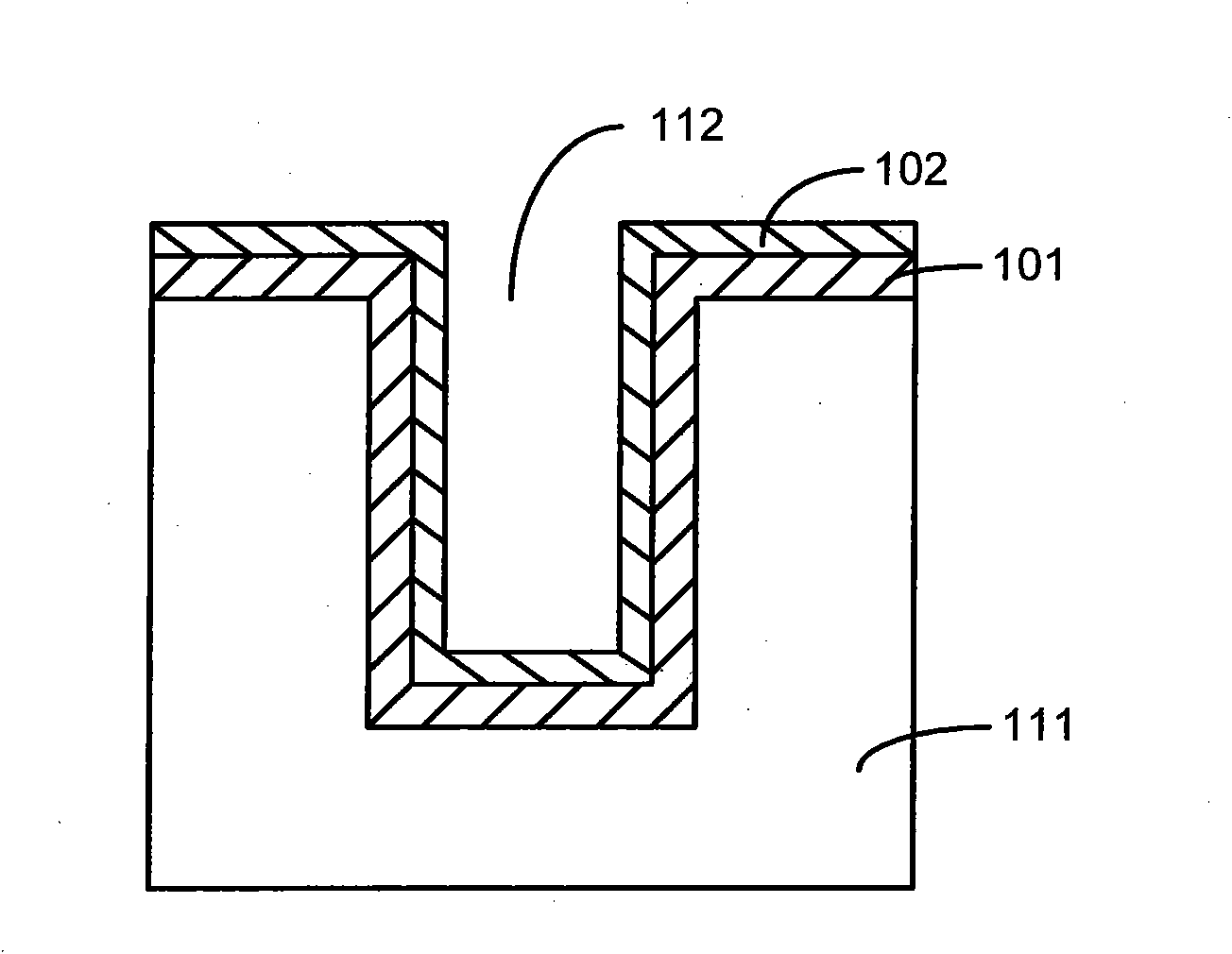
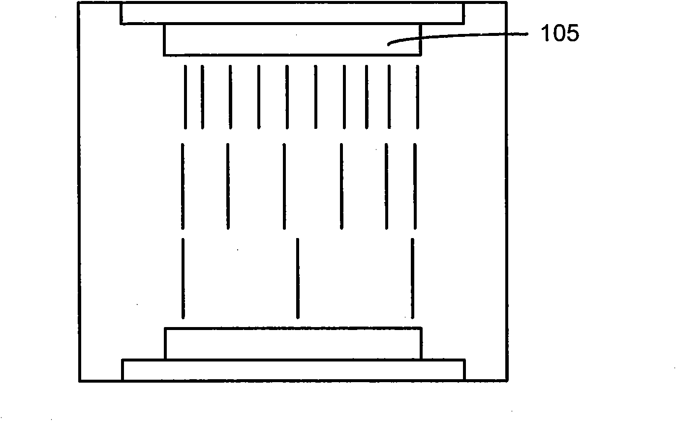
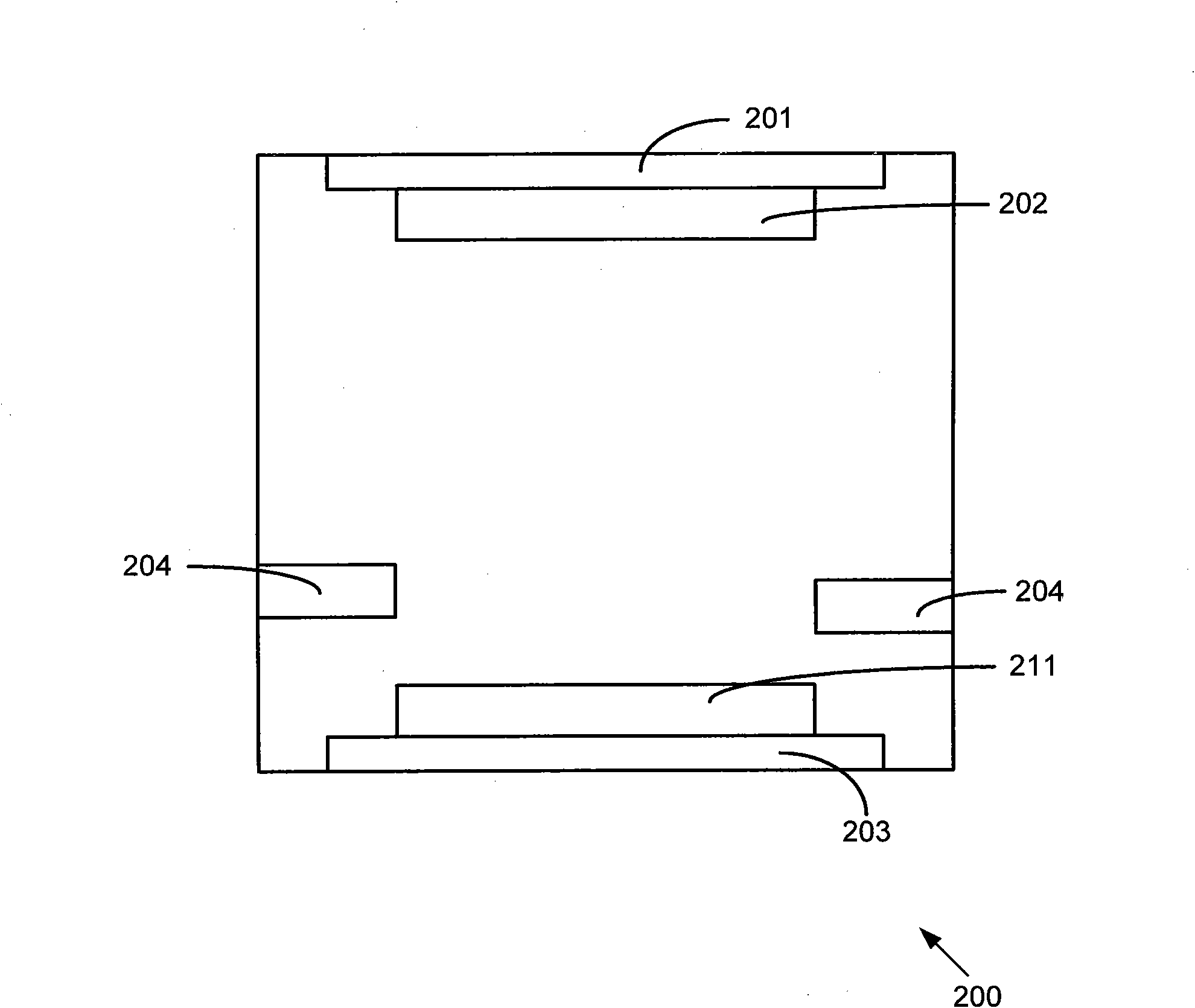
[0028] In the following description, numerous specific details are given in order to provide a more thorough understanding of the present invention. It will be apparent, however, to one skilled in the art that the present invention may be practiced without one or more of these details. In other examples, some technical features known in the art are not described in order to avoid confusion with the present invention.

[0029] In order to thoroughly understand the present invention, detailed steps will be presented in the following description to illustrate how the present invention fabricates the metal compound thin film. Obviously, the practice of the invention is not limited to specific details familiar to those skilled in the semiconductor arts. Preferred embodiments of the present invention are described in detail below, however, the present invention may have other embodiments besides these detailed descriptions.

[0030] In the following paragraphs the invention is des...


PUM

PropertyMeasurementUnit
thicknessaaaaaaaaaa

Abstract

The invention provides a method for forming metal compound film, which comprises the following steps: providing a front-end device structure, placing the front-end device structure at a bottom of a reaction chamber which comprises a sputtering device and an inductively coupled plasma device, wherein the sputtering device comprises a target located on the top of the reaction chamber, and the inductively coupled plasma device is used to form a plasma area on the surface of the front-end device structure; forming a target material film formed by the target material on the front-end device structure by the sputtering device; injecting reaction gas to allow the reaction gas to react with the target material film under the condition that the sputtering device is turned off and the inductively coupled plasma device is turned on so as to form the metal compound film. According to the invention, it is ensured that the formed target material film does not change performance of itself due to the containing of other impurities.

Description

technical field [0001] The invention relates to a semiconductor manufacturing process, in particular to a method for forming a metal compound thin film. Background technique [0002] The performance of high-end microprocessor chips is increasingly limited by signal propagation delays in the interconnect wiring used to maintain connections between devices in the chip. In interconnects commonly referred to as back-end-of-line (BEOL), the delay in these wires is represented by the product of resistance R and capacitance C associated therewith. With the continuous improvement of chip integration, copper has replaced aluminum as the mainstream interconnection technology in VLSI manufacturing. As a substitute for aluminum, copper wires can reduce interconnection impedance, reduce power consumption and cost, and improve chip integration, device density and clock frequency. When R is reduced by replacing aluminum with copper in BEOL wiring, the reduction in C can be achieved by re...

Claims


Application Information

Patent Timeline
Patent Type & Authority Applications(China)
IPC IPC(8): C23C14/34C23C14/35C23C14/06H01L21/768
Inventor 何伟业胡宇慧
Owner SEMICON MFG INT (SHANGHAI) CORP
Why Eureka
Try Eureka