
Solid-state imaging element, solid-state imaging device, solid-state imaging apparatus, and method for producing polarizing element

A solid-state photography element and solid-state photography technology, applied in the direction of polarizing elements, electric solid devices, electrical components, etc., can solve problems such as difficulties and inorganic particles, and achieve the effects of suppressing fading, excellent extinction characteristics, and suppressing mixing

Active Publication Date: 2012-04-04
SONY GRP CORP
View PDF12 Cites 19 Cited by
  • Summary
  • Abstract
  • Description
  • Claims
  • Application Information

AI Technical Summary

Problems solved by technology

Therefore, it is extremely difficult to form inorganic fine particles having different shape anisotropy in each solid-state imaging element
Therefore, it is extremely difficult to apply the polarizing element disclosed in Japanese Patent Laid-Open No. 2008-216956 to the technology disclosed in Non-Patent Document 1.

Method used


Image

  • Solid-state imaging element, solid-state imaging device, solid-state imaging apparatus, and method for producing polarizing element
  • Solid-state imaging element, solid-state imaging device, solid-state imaging apparatus, and method for producing polarizing element
  • Solid-state imaging element, solid-state imaging device, solid-state imaging apparatus, and method for producing polarizing element

Examples


Embodiment 1

[0070] 2. Embodiment 1 (solid-state imaging element of the present invention, solid-state imaging device of the present invention, imaging equipment, and method of manufacturing a polarizing element)

[0071] 3. Embodiment 2 (variation of the manufacturing method of the polarizing element of Embodiment 1)

[0072] 4. Embodiment 3 (variation of the manufacturing method of the polarizing element of Embodiment 2)

[0073] 5. Embodiment 4 (variation of Embodiment 1)

Embodiment 5

[0074] 6. Embodiment 5 (Modification of the solid-state imaging device of the present invention)

[0075] 7. Embodiment 6 (Modification of the solid-state imaging device of Embodiment 5)

[0076] 8. Embodiment 7 (another modification of the solid-state imaging device of Embodiment 5)

[0077] 9. Embodiment 8 (further modification of the solid-state imaging device of Embodiment 5)

[0078] 10. Embodiment 9 (further modification of the solid-state imaging device of Embodiment 5)

[0079] 11. Embodiment 10 (further modification of the solid-state imaging device of Embodiment 5)

[0080] 12. Embodiment 11 (further modification of the solid-state imaging device of Embodiment 5)

[0081] 13. Embodiment 12 (variation of Embodiment 11), others

[0082] [Description of the solid-state imaging element of the present invention, the solid-state imaging device, imaging equipment, and polarizing element of the present invention, and the overall description]

[0083]In the polarizing el...

Embodiment 2

[0227] Embodiment 2 is a modification of Embodiment 1. However, compared with the CVD method, the ADL method can perform film formation on the side surface of the polarizing element 70 more similarly. Therefore, it is possible to prevent reduction in the optical characteristics of the polarizing element. Especially due to AlO x and HfO x A protective film made of such a metal oxide has a high ability to protect a polarizing element, is thin, and can be formed similarly. Therefore, it can function as a high-quality protective film without causing a decrease in optical characteristics.

[0228] In Embodiment 2, the formation pitch P along the second direction is formed ab-2 =180nm, width W ab =80nm, polarizing element 70 and space between polarizing element 70 (P ab-2 -W ab )=100nm polarizing element 70. Specifically, in Example 2, in the same process as [Process-130] of Example 1, after removing the etching mask layer 92, the AlO x or HfO x The formed protective film 7...


PUM


Abstract

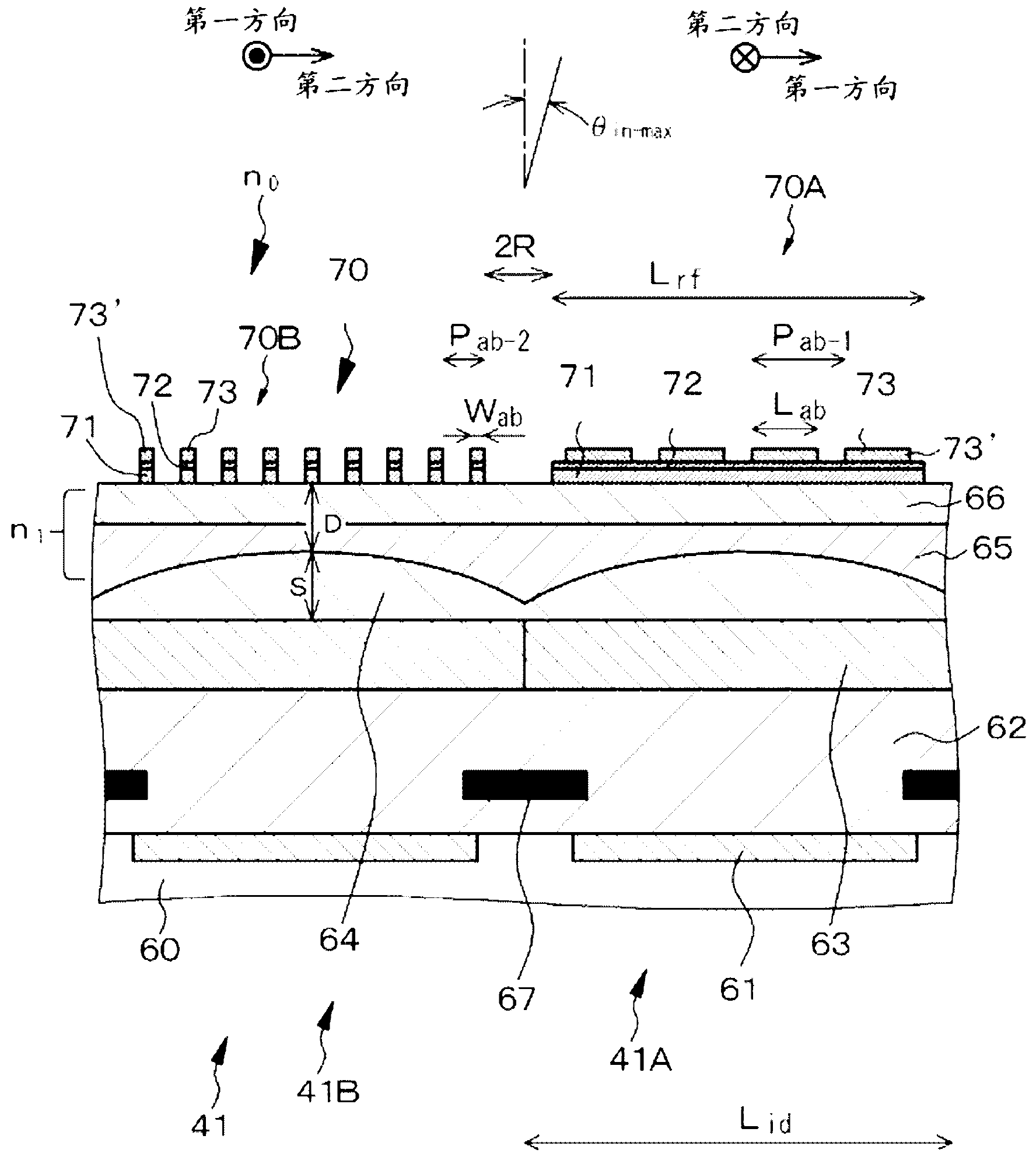
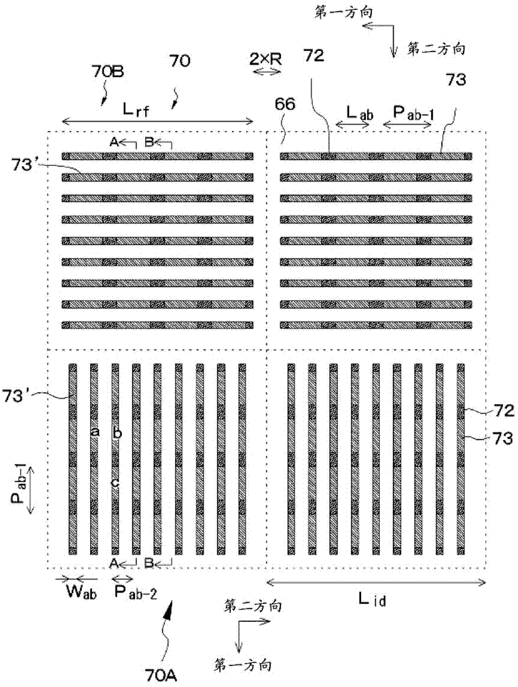
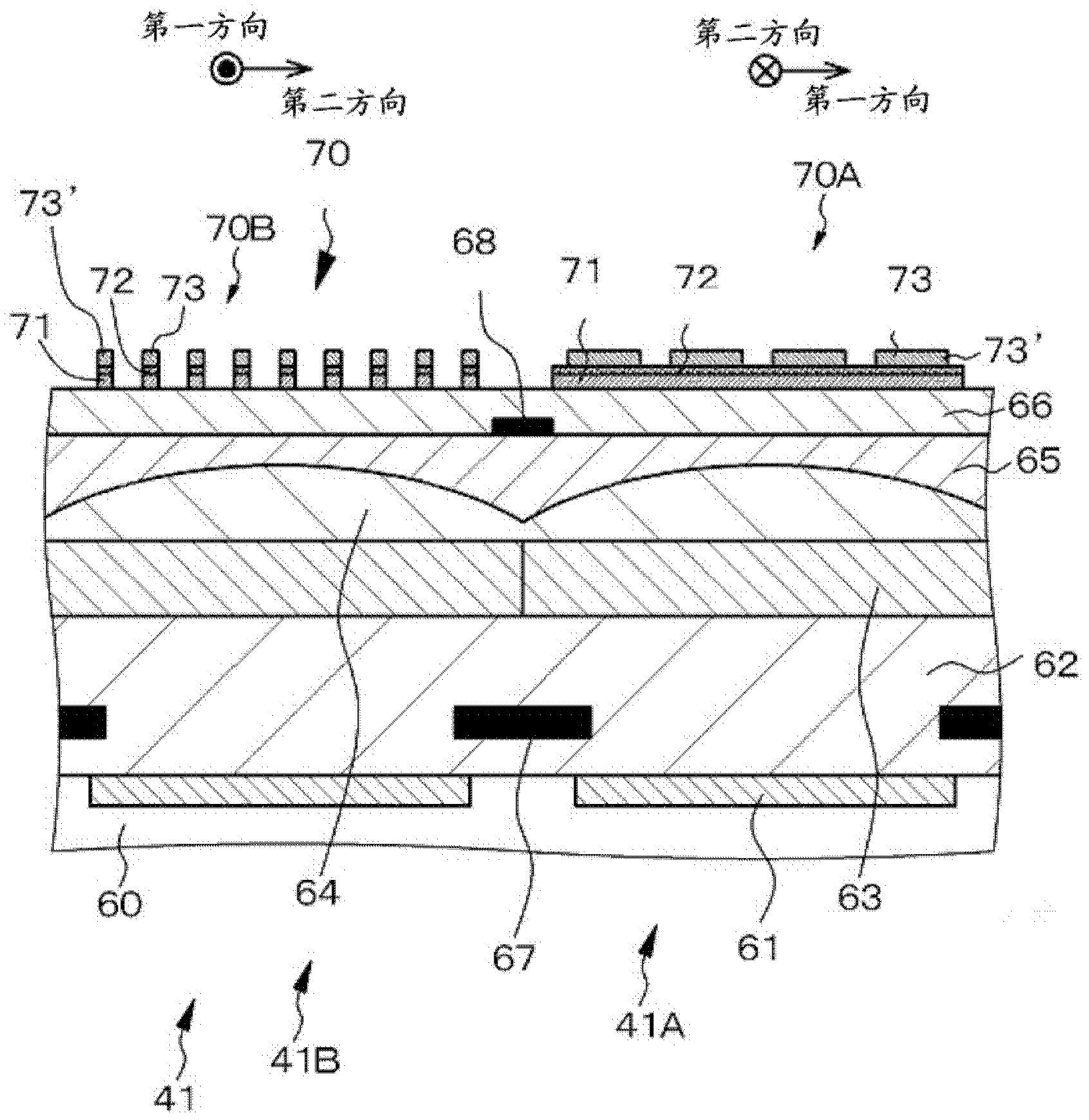
The present invention relates to: a solid-state imaging element which is capable of providing a solid-state imaging element that comprises a polarizing element which has simple configuration and structure based on wire grid polarizer technology; a solid-state imaging device; an imaging apparatus; and a method for producing a polarizing element. The solid-state imaging device comprises a plurality of solid-state imaging elements (41) each of which comprises a photoelectric conversion element (61) and a polarizing element (70) that is arranged on the light incident side of the photoelectric conversion element (61). The solid-state imaging device comprises two or more kinds of polarizing elements (70) that have different polarization directions, and each polarizing element has a lamination structure wherein a stripe-patterned reflective layer (71), an insulating layer (72) that is formed on the reflective layer (71) and a light absorption layer (73), which is composed of a plurality of pieces (73') that are formed on the insulating layer (72) so as to be separated from each other, are laminated from the photoelectric conversion element side.

Description

technical field [0001] The present invention relates to a solid-state imaging element, a solid-state imaging device, an imaging device, and a method of manufacturing a polarizing element. Background technique [0002] The commercialization of optical elements that change the polarization direction and arrange polarizing elements in every minute area, and electronic devices integrating such optical elements is being promoted centering on display devices and measurement devices. Xpol (registered trademark) manufactured by Arisawa Seisakusho. [0003] In addition, Japanese Patent Application Laid-Open No. 2004-309868 discloses a photographing device comprising: a photographing device provided with pixels equivalent to an integer multiple of a predetermined number of scanning lines on the photographing surface; The first horizontal component polarization means of the horizontal component of the light is arranged at a position separated from the first horizontal component polari...

Claims


Application Information

Patent Timeline
Patent Type & Authority Applications(China)
IPC IPC(8): G03B17/12G02B5/30H01L27/146G02B30/25
CPCH01L27/14621H01L27/14625H01L27/14627H01L27/14629H01L27/14605H01L27/146G02B5/30
Inventor 小泽谦
Owner SONY GRP CORP
Learn More