Preparation method of TEM (Transmission Electron Microscopy) sample

A sample and sample technology, which is applied in the field of TEM sample preparation, can solve the problems of unclear contact hole pattern and inability to accurately observe the contact hole shape, and achieve the effect of easy observation and high accuracy

Active Publication Date: 2012-04-11
SEMICON MFG INT (SHANGHAI) CORP +1
View PDF5 Cites 17 Cited by
  • Summary
  • Abstract
  • Description
  • Claims
  • Application Information

AI Technical Summary

Problems solved by technology

[0009] However, when the sample formed by the above method is observed by TEM, if the pattern to be detected is a contact hole, then as Figure 4b In the crystalline phase diagram of the TEM sample shown, the pattern of the contact hole is not clear, so the morphology of the contact hole cannot be accurately observed

Method used


Image

  • Preparation method of TEM (Transmission Electron Microscopy) sample
  • Preparation method of TEM (Transmission Electron Microscopy) sample
  • Preparation method of TEM (Transmission Electron Microscopy) sample

Examples


preparation example Construction

[0035] Figure 5 It is a flowchart of the preparation method of the TEM sample of the present invention. Such as Figure 5 Shown, the preparation method of TEM sample of the present invention comprises steps:

[0036] S10, providing a test sample, the test sample has a contact hole and a metal layer on both sides of the contact hole, and the metal layer is connected to the filling metal in the contact hole through a metal connection;

[0037] S20, cutting out a sample from the test sample, the sample including the contact hole, the metal wiring and the metal layer;

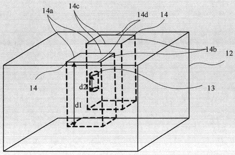
[0038] S30, forming pits on both sides of the contact hole, the metal interconnection and the metal layer on the front surface of the sample, the pit having an opposite surface opposite to the contact hole, the metal interconnection and the metal layer;

[0039] S40, thinning the thickness of the area where the contact hole and part of the metal wiring of the sample are located from the opposite surface of the pi...


PUM

PropertyMeasurementUnit
thicknessaaaaaaaaaa
thicknessaaaaaaaaaa
thicknessaaaaaaaaaa

Abstract

The invention provides a preparation method of a TEM (Transmission Electron Microscopy) sample. The preparation method comprises the following steps of: providing a detecting sample wafer which is provided with a contact hole and metal layers arranged at two sides of the contact hole, wherein the metal layers are connected with a filling metal in the contact hole through a metal connecting wire; cutting a sample wafer from the detecting sample wafer, wherein the sample wafer comprises the contact hole, the metal connecting wire and the metal layers; forming pits at two sides of the contact hole, the metal connecting wire and the metal layers on the frontage of the sample wafer, wherein the pit is provided with an opposite surface opposite to the contact hole, the metal connecting wire andthe metal layers; thinning the thickness of a region at which the contact hole and partial metal connecting wire of the sample wafer are located from the opposite surface of the pit; cutting off the sample wafer between the pits, wherein the cut-off part comprises the thinned region and un-thinned regions provided with the metal layers and arranged at two sides of the thinned region, thereby improving the accuracy of the TEM observation.

Description

technical field [0001] The invention relates to the technical field of semiconductor manufacturing, in particular to the field of sample preparation methods for TEM (Transmission Electron Microscope). Background technique [0002] In the semiconductor manufacturing industry, there are a variety of inspection equipment, among which EM is an important tool for inspecting the morphology, size and characteristics of the thin films that make up the device. Commonly used EMs include TEM (Transmission Electron Microscope) and SEM (Scanning Electron Microscope). The working principle of TEM is to thin the sample to be tested by cutting, grinding, ion thinning, etc., and then put it into the TEM observation room, irradiate the sample with a high-voltage accelerated electron beam, enlarge the shape of the sample, and project it on the screen. One of the outstanding advantages of TEM is that it has a high resolution and can observe the shape and size of extremely thin films. [0003]...

Claims


Application Information

Patent Timeline
Patent Type & Authority Applications(China)
IPC IPC(8): G01N1/28
Inventor 段淑卿庞凌华陈柳王玉科陈祯祥
Owner SEMICON MFG INT (SHANGHAI) CORP
Why Eureka
Try Eureka