
Ceramic multilayer substrate producing method

A technology of multilayer substrate and manufacturing method, which is applied in the direction of multilayer circuit manufacturing, printed circuit manufacturing, and electric recording technology using charge patterns, etc., can solve the problem of surface electrodes such as ceramic multilayer substrates, and achieve the suppression of migration intensification, Effect of preventing short circuit between electrodes

Inactive Publication Date: 2012-04-11
MURATA MFG CO LTD
View PDF6 Cites 4 Cited by
  • Summary
  • Abstract
  • Description
  • Claims
  • Application Information

AI Technical Summary

Problems solved by technology

[0011] The object of the present invention is to provide a method of manufacturing a ceramic multilayer substrate that can solve the problem of surface electrodes caused by toner exposure as described above.

Method used


Image

  • Ceramic multilayer substrate producing method
  • Ceramic multilayer substrate producing method
  • Ceramic multilayer substrate producing method

Examples


Embodiment approach 1

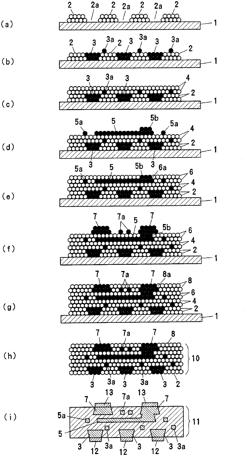
[0036] figure 1 Embodiment 1 which shows the manufacturing process of a ceramic multilayer board|substrate. This embodiment relates to a method of forming both the ceramic layer and the electrode using electrophotography as a method of directly forming the ceramic layer and the electrode on the carrier member (direct transfer method). Hereinafter, the manufacturing process will be described in the order of lamination.

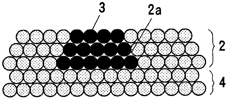
[0037] figure 1 (a) shows the state where the outer layer ceramic layer 2 is formed on the carrier member 1 by electrophotography using a ceramic toner (charged powder for forming a ceramic layer). The carrier member 1 may be a resin film having heat resistance above the fixing temperature, such as a PET film, or may be a thin metal plate. On the outer ceramic layer 2, an opening 2a having the same size as a surface electrode to be formed later is formed.

[0038] One example of a specific method of forming the ceramic layer 2 is as follows.

[0039] (1)...

Embodiment approach 2

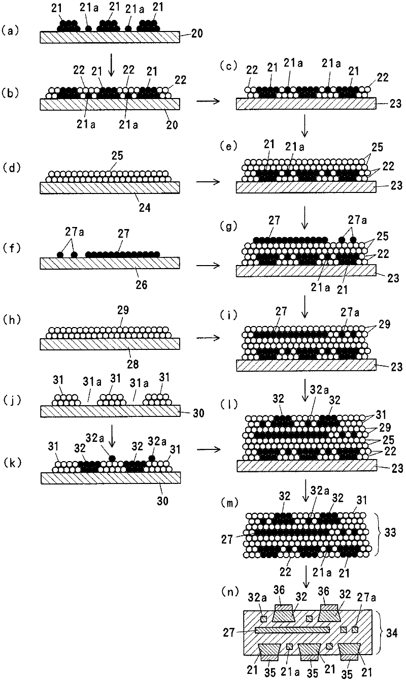
[0092] image 3 Embodiment 2 which shows the manufacturing process of a ceramic multilayer board|substrate. This embodiment relates to a method of forming both a ceramic layer and an electrode using an electrophotography method as a method of transferring a ceramic layer and an electrode onto a carrier member using an intermediate transfer body (intermediate transfer method). Hereinafter, the manufacturing process will be described in the order of lamination.

[0093] image 3 (a) shows the state where the surface electrode 21 was formed on the intermediate transfer body (for example, PET film) 20 using the electrode toner by electrophotography. Here, the exposure toner 21 a generated near the surface electrode 21 runs onto the intermediate transfer body 20 . The method of forming the surface electrodes 21 and the material of the electrode toner are the same as those in the first embodiment.

[0094] image 3 (b) shows the state where the outer layer ceramic layer 22 is f...

Embodiment approach 3

[0109] Figure 4 Embodiment 3 of the manufacturing method of a ceramic multilayer substrate is shown. This embodiment relates to a method using a ceramic green sheet as a method of directly forming a ceramic layer and an electrode on a carrier member (direct transfer method). Hereinafter, the manufacturing process will be described in the order of lamination.

[0110] Figure 4 (a) shows a state where the pattern of the outer ceramic layer 41 is formed on the carrier member 40 using a ceramic green sheet. On the outer ceramic layer 41, an opening 41a having the same size as a surface electrode formed later is formed. As a method for forming the opening, a known method can be used, for example, forming a hole with a mechanical punch or using a screen printing method.

[0111] One example of a method of forming the outer ceramic layer 41 is as follows.

[0112] (1) For ceramic materials, use a material (BAS material) composed of components centered on Ba, Al, and Si, blend ...


PUM

PropertyMeasurementUnit
thicknessaaaaaaaaaa

Abstract

When electrodes are formed on the front and back main surfaces of a ceramic multilayer substrate by xerography, faults generated by fog toner are improved. A first outer layer ceramic layer which has openings at locations in which surface electrodes should be formed is formed on a carrier member, and surface electrodes are formed in the openings of the outer layer ceramic layer by xerography, using electrode toner. Further, after a laminated body is obtained by alternately forming inner layer ceramic layers and inner electrode patterns on the first outer layer ceramic layer and the surface electrodes, back surface electrodes are formed on the laminated body by xerography, using the electrode toner. After that, a second outer layer ceramic layer is formed so as to bridge the area other than the back surface electrodes, and the laminated body is removed from the carrier member, and is sintered to obtain a ceramic multilayer substrate. Thus, the fog toner generated when the front and back surface electrodes are formed is covered by the outer layer ceramic layer. Accordingly, the short circuit between the electrodes or the deterioration of IR can be resolved.

Description

technical field [0001] The present invention relates to a method for manufacturing a ceramic multilayer substrate having electrodes formed on both front and back surfaces, and more particularly to a method for manufacturing a ceramic multilayer substrate in which electrodes are formed by electrophotography. Background technique [0002] Conventionally, electrophotography is known as a new circuit forming method instead of the wiring printing method using a screen mask. This method is to form a charge image (electrostatic latent image) in the shape of an electrode pattern on the surface of the photoreceptor, to make the charged powder (electrode toner) for forming the electrode adhere to the electrostatic latent image electrostatically, and to attach the electrode in the shape of the electrode pattern to the surface of the photoreceptor. An image generated by the toner is transferred onto a ceramic green sheet and then fixed (for example, refer to Patent Document 1). [0003...

Claims


Application Information

Patent Timeline
Patent Type & Authority Applications(China)
IPC IPC(8): H05K3/46H05K3/12H05K3/18
CPCH05K3/4682H05K3/246H05K3/1266H05K3/4667H05K1/0306H05K2201/09881H05K2203/0517B33Y80/00G03G15/224G03G15/6585G03G15/6591
Inventor 山元一生岩越邦男镰田明彦
Owner MURATA MFG CO LTD
Learn More