
Liquid crystal display device

A liquid crystal display device and liquid crystal technology, which are applied in the directions of identification devices, filters, optics, etc., can solve the problems of uneven display and increase, and achieve the effect of excellent display quality.

Inactive Publication Date: 2012-04-18
TOPPAN PRINTING CO LTD
View PDF5 Cites 9 Cited by
  • Summary
  • Abstract
  • Description
  • Claims
  • Application Information

AI Technical Summary

Problems solved by technology

Increased display unevenness due to a significant change in light transmittance in the upper edge portion protruding outside the light-shielding area compared to other portions

Method used


Image

  • Liquid crystal display device
  • Liquid crystal display device
  • Liquid crystal display device

Examples


no. 1 approach

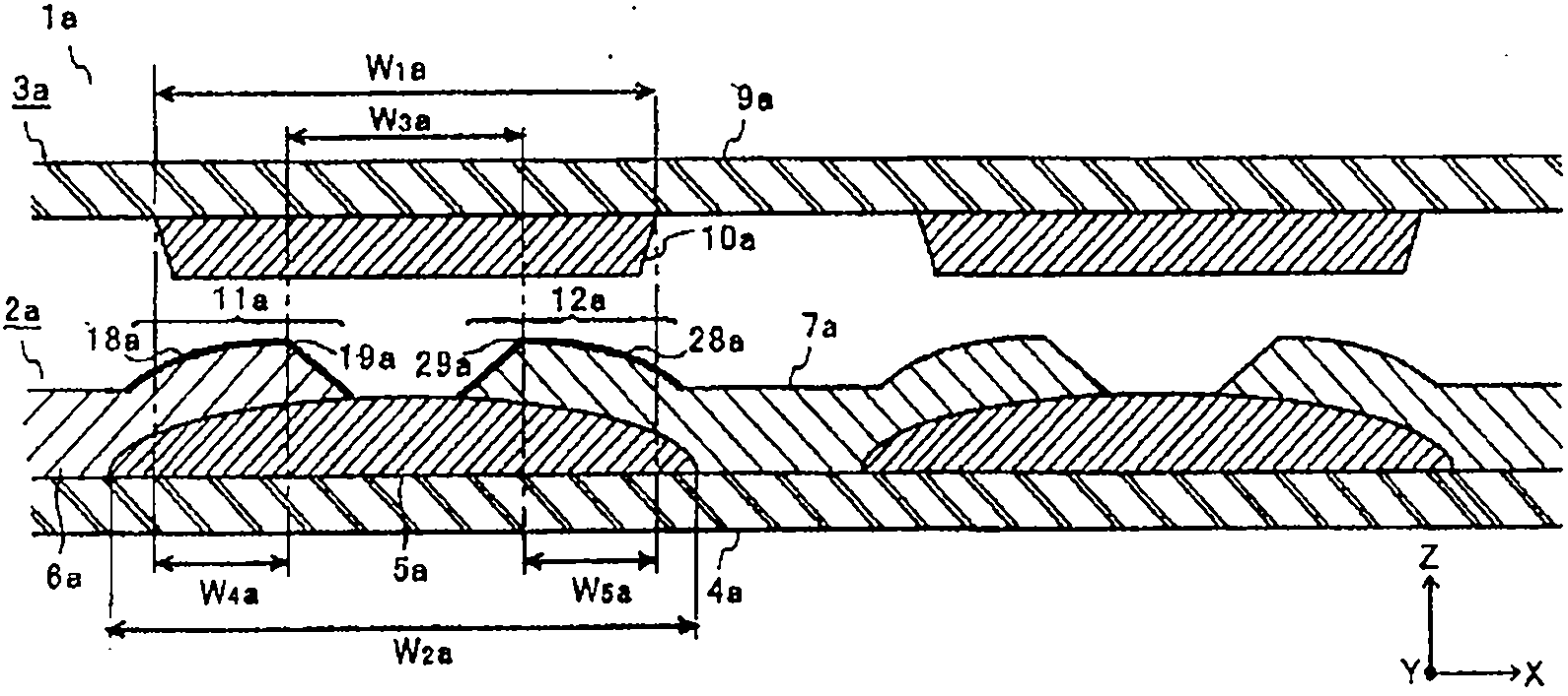
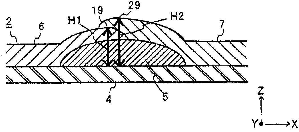
[0031] figure 1 is a cross-sectional view showing a schematic configuration of a liquid crystal display device according to a first embodiment of the present invention, figure 2 It is a sectional view explaining the position of the upper end edge of the protrusion of another example.

[0032] The liquid crystal display device 1a of the first embodiment has a plurality of pixels arranged in the directions of the X-axis and the Y-axis, and includes a color filter 2a and a TFT substrate 3a that are attached to each other, and a pixel that is sealed and formed between them. Slit liquid crystal (not shown). On the outside of the TFT substrate 3a ( figure 1 above), a light source not shown in the figure is arranged.

[0033] The color filter 2a includes a substrate 4a, a black matrix 5a disposed on the substrate 4a, and a plurality of colored layers 6a and 7a formed at each pixel position. The colored layers 6a and 7a constitute overlapping portions 11a and 12a that partially...

no. 2 approach

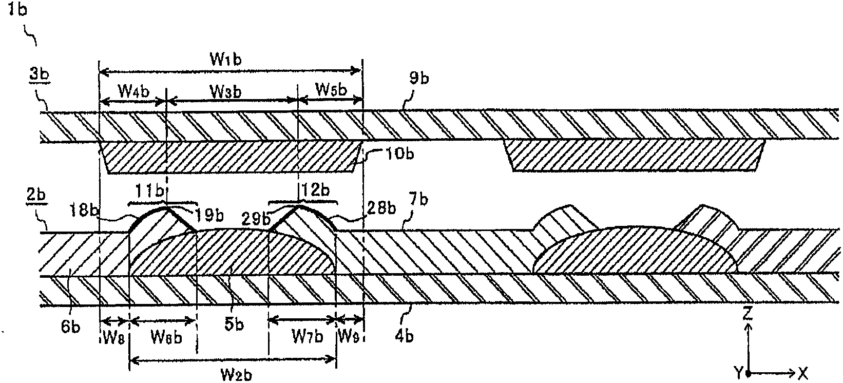
[0043] image 3 It is a cross-sectional view showing a schematic configuration of a liquid crystal display device according to a second embodiment of the present invention.

[0044] The liquid crystal display device 1b of the second embodiment differs from the liquid crystal display device of the first embodiment in that the area where the overlapping portion of the colored layer and the black matrix is ​​shielded is different. Specifically, the entire overlapping portion is shielded from light by the light shielding portion.

[0045] In the second embodiment, the width W of the light shielding portion 10b 1 b is set to be greater than the width W of the black matrix 5 2 b, overlapping portions 11b and 12b are shielded from light by the light shielding portion 10b. Specifically, the overlapping portions 11b and 12b are disposed on the inside of a line projecting the edge of the light shielding portion 10b in the X-axis direction onto the substrate 4b. In addition, since th...

Embodiment

[0051] Hereinafter, examples for implementing the present invention will be described.


PUM


Abstract

Disclosed is a liquid crystal display device free of display variation due to the misalignment and assembling error of an exposure head and excellent in display quality. The liquid crystal display device (1) is provided with a color filter (2), a TFT substrate (3) so joined to the color filter (2) as to face the color filter (2), and a liquid crystal (not shown) sealed in the space defined therebetween. The color filter (2) includes a substrate (4), a black matrix (5) disposed on the substrate (4), and a plurality of colored layers (6, 7) overlapping the black matrix (5) in the pixel positions. Upper end edges (19a, 29a) where the vertexes of ridges (18a, 28a) formed by the overlap of the colored layers (6, 7) and the black matrix (5) continuously range in the Y-axis direction are positioned in the region shielded against light by a light-shielding section (10a) of the TFT substrate (3).

Description

technical field [0001] The invention relates to a liquid crystal display device formed by sealing liquid crystal between a color filter and a thin film transistor (TFT) substrate. Background technique [0002] A color filter used in a liquid crystal display device includes colored layers of three colors of red, green, and blue constituting pixels on a substrate, and a black matrix provided between each pixel to shield light. A TFT substrate having a plurality of thin film transistors (including pixel electrodes, switching elements made of semiconductors, and an insulating film layer), source wiring, and gate wiring is arranged opposite to the color filter, and is sealed between them. liquid crystal. [0003] In the manufacturing process of the color filter, the coloring layer and the black matrix are patterned by photolithography. In this case, an exposure method using a plurality of small photomasks (hereinafter referred to as "Small mask continuous exposure method"). ...

Claims


Application Information

Patent Timeline
Patent Type & Authority Applications(China)
IPC IPC(8): G02F1/1335G02B5/00G02B5/20G02F1/1368G09F9/30G09F9/35
CPCG02F1/133514G02B5/201G02F1/133512G02F2001/13625G02F1/13625G02B5/003G02F1/133516G02F1/136286
Inventor 松井浩平八田薰
Owner TOPPAN PRINTING CO LTD
Learn More