
Source region of LDMOS (Laterally Diffused Metal Oxide Semiconductor) device and manufacturing method thereof

A source region and device technology, used in semiconductor/solid-state device manufacturing, semiconductor devices, electrical components, etc., can solve the problems of weakness, uneven doping at both ends, and limited breakdown voltage of LDMOS devices, and achieve improved breakdown. The effect of voltage

Active Publication Date: 2013-03-13
SHANGHAI HUAHONG GRACE SEMICON MFG CORP
View PDF0 Cites 0 Cited by
  • Summary
  • Abstract
  • Description
  • Claims
  • Application Information

AI Technical Summary

Problems solved by technology

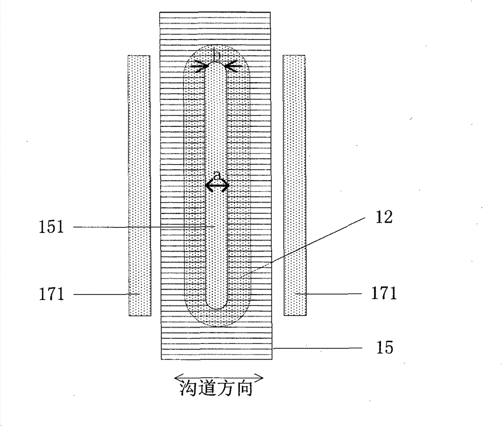
Apparently, the ion implantation process with an oblique angle has a shadow effect of ion implantation in the region at both ends of the cavity 151, which will lead to uneven doping at both ends of the formed p-well 172, and even weak spots, which eventually lead to LDMOS The breakdown voltage of the device is limited

Method used


Image

  • Source region of LDMOS (Laterally Diffused Metal Oxide Semiconductor) device and manufacturing method thereof
  • Source region of LDMOS (Laterally Diffused Metal Oxide Semiconductor) device and manufacturing method thereof
  • Source region of LDMOS (Laterally Diffused Metal Oxide Semiconductor) device and manufacturing method thereof

Examples


Embodiment Construction

[0033] The present invention will be described below by taking n-type LDMOS as an example. The present invention is also applicable to p-type LDMOS, and it only needs to reverse the doping types of each part in n-type LDMOS.

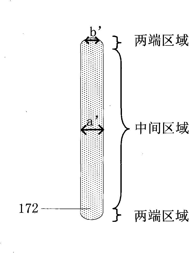
[0034] see Figure 4a , which is a schematic diagram of the layout of the source region of the LDMOS of the present invention. The source region of the LDMOS is the p-well 172 , which is generally dumbbell-shaped, including a rectangular middle region and polygonal two-end regions. The width of the middle region of the rectangle along the direction of the channel is a', which is the short side dimension of the rectangle. The minimum width of the two ends of the polygon along the channel direction is c', the maximum width is e', c'≥a', 1.5a'≤e'≤2a'. The minimum width of the area at both ends of the polygon in the direction of the vertical channel is d', the maximum width is f', d'≥a', 1.5a'≤f'≤2a'.

[0035] The improvement of the present invention to t...


PUM


Abstract

The invention discloses a source region of an LDMOS (Laterally Diffused Metal Oxide Semiconductor) device, which is in the shape of a dumbbell. The source region comprises a rectangular intermediate region and two polygonal terminal regions, wherein the spacing of the rectangular intermediate region of the source region in the channel direction is a'; the minimum spacing of each polygonal terminal region of the source region in the channel direction is c', the minimum spacing in the direction perpendicular to the channel direction is d', c'>=a', and d'>=a'. The invention also discloses a manufacturing method of the source region of the LDMOS. By changing the two terminal regions of the source region of the LDMOS device from the traditional semicircles to polygons, the invention ensures that the ion implantation shadow effect can not be produced in the source region manufacturing process, thereby being beneficial to improving the breakdown voltage of the LDMOS device.

Description

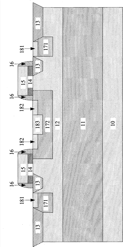
technical field [0001] The invention relates to an LDMOS (laterally diffused MOS, laterally diffused MOS transistor) device. Background technique [0002] see figure 1 , which is a schematic cross-sectional view of an existing LDMOS. There is an n-type buried layer 11 on the p-type substrate 10 , and there is an n-well 12 further above. The depth of the n-well 12 is usually greater than 2 μm, and is also called a deep n-well. There are multiple isolation regions 13 in the n well 12, and these isolation regions 13 isolate the n well 171 and the p well 172 in the n well 12 from each other. There is an n-type heavily doped region 181 in the n well 171, which serves as the drain of the LDMOS device. The p-well 172 has an n-type heavily doped region 182 and a p-type heavily doped region 183, which are connected to serve as the source of the LDMOS device. The p-well 172 is the source region of the LDMOS device. There is a gate oxide layer 14 on the n-well 12, and a gate 15 o...

Claims


Application Information

Patent Timeline
Patent Type & Authority Patents(China)
IPC IPC(8): H01L29/78H01L29/06H01L29/423H01L21/336H01L21/265
Inventor 张帅戚丽娜
Owner SHANGHAI HUAHONG GRACE SEMICON MFG CORP
Learn More