High voltage diode assembly tool and operation method thereof

A technology for high-voltage diodes and assembly fixtures, which is applied in the fields of electrical components, semiconductor/solid-state device manufacturing, and circuits. The effect of production operations

Active Publication Date: 2013-05-01
YANGZHOU YANGJIE ELECTRONIC TECH CO LTD
View PDF4 Cites 0 Cited by
  • Summary
  • Abstract
  • Description
  • Claims
  • Application Information

AI Technical Summary

Problems solved by technology

Calculated on an 8-hour working day, each person can only complete 20,000 chip identifications in one shift, and the labor efficiency is low
And because the chip size is small (1-5mm), the labor intensity of the operator is extremely high, and it is easy to make work mistakes due to fatigue

Method used


Image

  • High voltage diode assembly tool and operation method thereof
  • High voltage diode assembly tool and operation method thereof
  • High voltage diode assembly tool and operation method thereof

Examples


Embodiment Construction

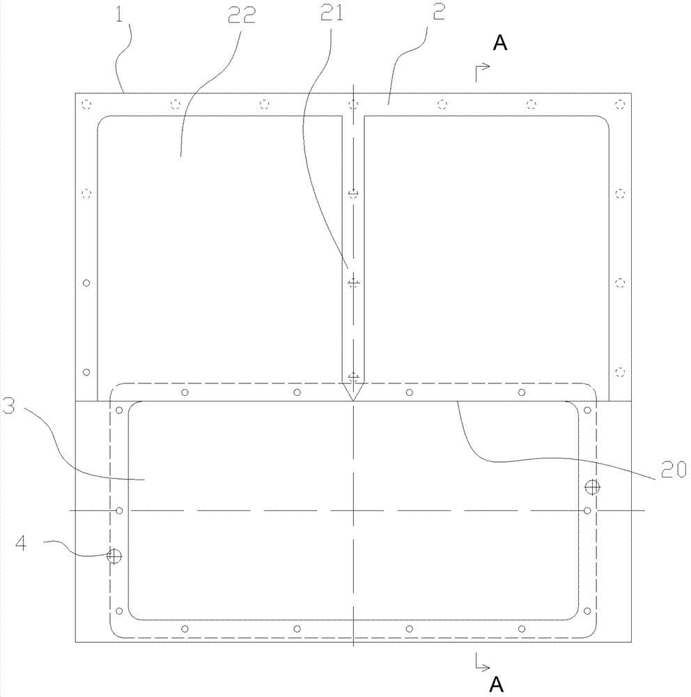
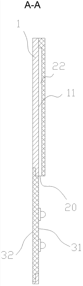
[0027] The present invention as Figure 1-5 As shown, it includes a chip chuck 5 and a conversion board, the conversion board includes a base plate 1 and a cover plate 2, the cover plate 2 is fixedly connected to the top surface of the base plate 1 as the working surface 11, and the cover plate 2. The area is smaller than the area of ​​the top surface of the substrate 1, so that an exposed working surface portion 31 is left on the top surface of the substrate 1; a gap 22 is left between the cover plate 2 and the substrate 1, and the opening 20 of the gap faces The exposed working surface part 31 part; the height of the gap 22 is less than the width and length of the chip 6, so that the chip 6 will not turn over in the gap 22;

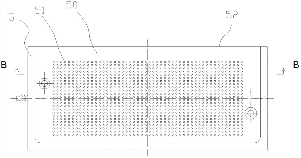
[0028] The chip chuck 5 has a shape matching the plane profile of the exposed working surface portion 31, and the surface of the chip chuck 5 facing the exposed working surface portion 31 is provided with a sinking surface 50, and the sinking surface 50...


PUM


Abstract

The invention provides a high voltage diode assembly tool and an operation method thereof. The invention relates to a special-purpose assembly tool of a high voltage diode chip and an operation method thereof. The invention provides a chip capable of mass arrangement, the high voltage diode assembly tool with convenient operation and the operation method thereof. The tool comprises a chip sucker and a conversion plate. The conversion plate comprises a substrate and a cover plate. The cover plate is fixedly connected to the substrate as a top surface of a working face. An area of the cover plate is smaller than an area of the substrate top surface. The top surface of the substrate has an exposed working face part. Gap is provided between the cover plate and the substrate. An opening of thegap faces the exposed working face part. Height of the gap is less than width and length of the chip. The operating method of the present invention comprises the following steps: (1) loading; (2) connecting the chip sucker; (3) converting; (4) returning material. The tool of the present invention has the advantages of good maneuverability, convenient assembly, cleanness, small volume, and light weight, and is easy to realize continuous production work.

Description

technical field [0001] The invention relates to a special assembly jig for a high-voltage diode chip and an operation method thereof. Background technique [0002] At present, the high-voltage diode assembly fixture adopts the general sucker design, and the positive electrode of the chip is marked by color, and manually flipped on the chip sucker to make the polarity of the chip consistent, and then the chip assembled on the chip sucker is reversed to the upper part of the welding groove. Make several chips neatly into the groove. Calculated on an 8-hour working system, each person can only complete 20,000 chip identifications in one shift, and the labor efficiency is low. And because the chip size is small (1-5mm), the labor intensity of the operator is extremely high, and it is very easy to make work mistakes due to fatigue. Contents of the invention [0003] Aiming at the above problems, the present invention provides a high-voltage diode assembling jig and an operati...

Claims


Application Information

Patent Timeline
Patent Type & Authority Patents(China)
IPC IPC(8): H01L21/67H01L21/50
Inventor 王永彬
Owner YANGZHOU YANGJIE ELECTRONIC TECH CO LTD
Why Eureka
Try Eureka