Testing method and testing probe platform for image sensor chip

A technology of image sensor and test method, applied in the parts, instruments, measuring electricity and other directions of electrical measuring instruments, can solve the problems of decreased yield rate, poor positioning accuracy, long auxiliary time of pick and place action, etc.

Active Publication Date: 2012-05-02
JIAXING JINGYAN INTELLIGENT EQUIP TECH
View PDF7 Cites 26 Cited by
  • Summary
  • Abstract
  • Description
  • Claims
  • Application Information

AI Technical Summary

Problems solved by technology

[0012] During the CIS chip testing process, the CIS chip is placed in a single piece in the tray, and the chip needs to be picked and placed repeatedly for each test piece, which is easy to damage the chip, resulting in the possibility of a drop in yield, and poor positioning accuracy. The test machine often has abnormal handling, and the pick-and-place action requires a long auxiliary time, so the test efficiency of the test machine is also very low

Method used


Image

  • Testing method and testing probe platform for image sensor chip
  • Testing method and testing probe platform for image sensor chip
  • Testing method and testing probe platform for image sensor chip

Examples


Embodiment Construction

[0026] The present invention will be described in detail below through embodiments in conjunction with the accompanying drawings.

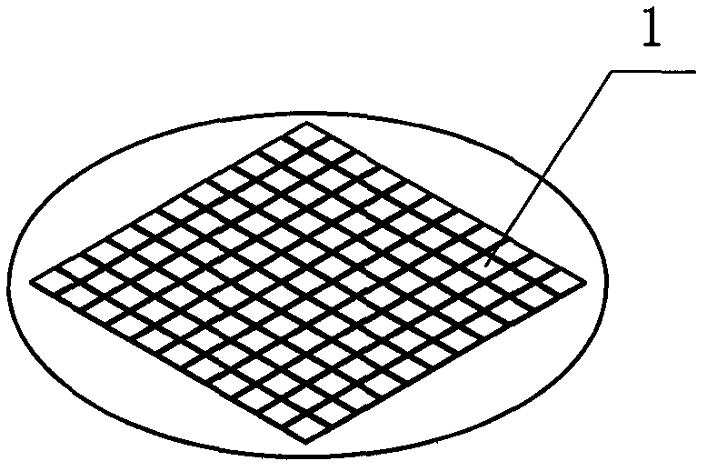
[0027] The test method for testing the image sensor chip is that the chip of the image sensor to be tested is composed of a plurality of chips 1 to form a wafer 2 such as figure 1 carried out in the state shown. It is tested under the condition that the chip 1 of the image sensor under test is packaged and still in the state of the wafer 2 after the electrical performance test.

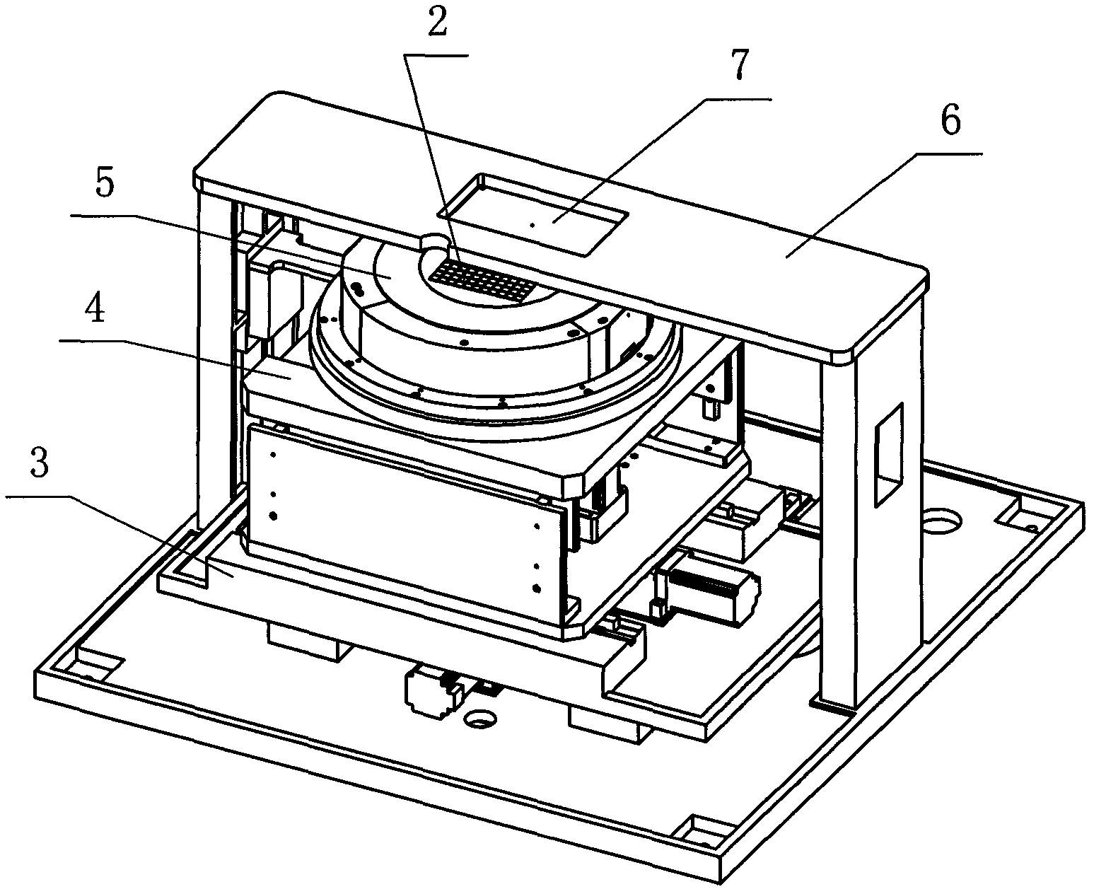
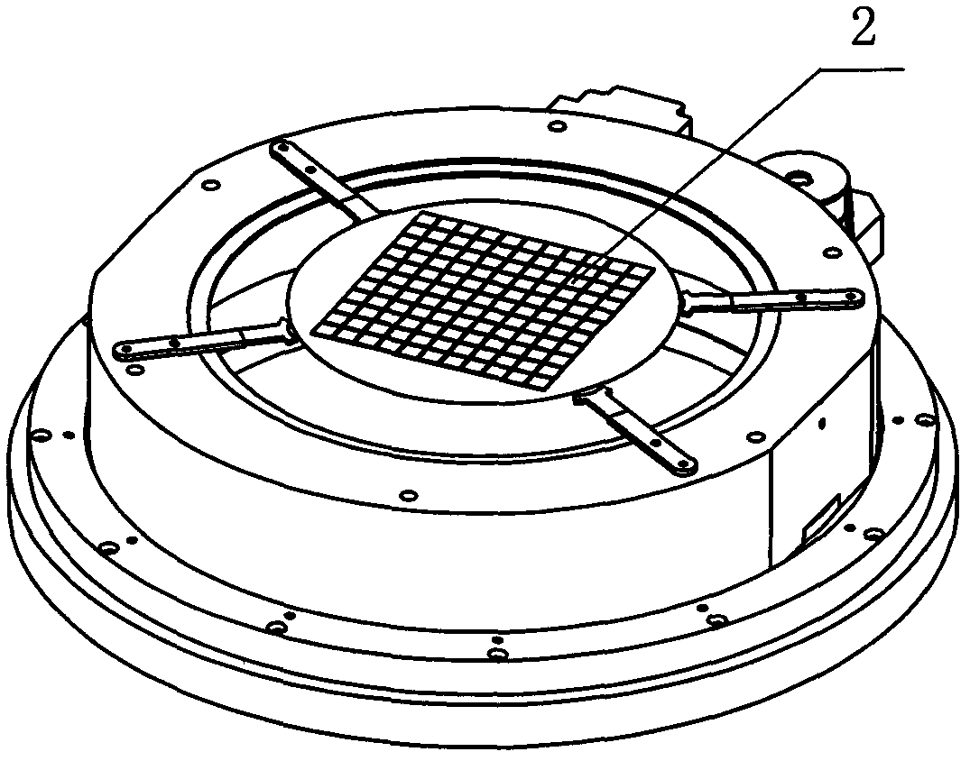
[0028] Utilize the probe station designed by the testing method of above-mentioned testing image sensor chip as figure 2 , 3 , 4, including an XY platform 3 that can move back and forth, left and right, and an elevating platform 4 that can move up and down is installed on the XY platform 3, and the elevating platform 4 is equipped with a wafer 2 for placing and can be used for circumferential rotation The chip carrier 5 is provided with a support frame 6 above the chi...


PUM


Abstract

The invention discloses a testing method and a testing probe platform for an image sensor chip and aims to provide a testing method for a contact image sensor (CIS) chip and a probe platform for testing the performance of the image sensor, which have the advantages of simple structure, high universality, low input cost and high testing efficiency. Testing on the image sensor chip to be tested is performed under the state that a plurality of chips are combined to form a wafer. The probe platform designed by utilizing the testing method for the image sensor chip comprises an XY platform capable of horizontally moving front and back and left and right; the XY platform is provided with a lifting platform capable of vertically moving; the lifting platform is provided with a wafer carrying disk which is used for containing the wafer and is capable of rotating in the circumferential direction; and a probe clip is arranged above the wafer carrying disk through a support frame in the manner of suspension. The testing probe platform is characterized in that a light source for generating light is arranged in the lifting platform below the wafer carrying disk. The testing method and the testing probe platform for the image sensor chip are capable of reducing damage to the CIS chip while ensuring the positioning accuracy, and is capable of greatly improving the degree of automation and the efficiency of the testing.

Description

technical field [0001] The invention relates to a test method for an image sensor (CIS) chip and a probe platform for testing the image sensing performance of the image sensor (CIS) chip manufactured by the test method. Background technique [0002] The probe station is a kind of equipment used for wafer testing in the semiconductor production process. It is mainly used as a precision positioning unit to complete the reliable contact between the probe card and the wafer in the wafer test and the signal connection between the probe station and the testing machine. Functions, etc., are called the central measurement and control needle platform, and its realization steps are as follows: [0003] 1. Place a silicon wafer with multiple chips arranged and connected together on the probe station; [0004] 2. The motor controls the XY positioning to the motion platform, so that one of the semiconductor chips to be tested in the silicon wafer is located directly under the probe card...

Claims


Application Information

Patent Timeline
Patent Type & Authority Applications(China)
IPC IPC(8): G01R1/02
Inventor 朱玉萍岑刚
Owner JIAXING JINGYAN INTELLIGENT EQUIP TECH
Why Eureka
Try Eureka