Method for selectively growing nickel

A selective, seed layer technology, applied in liquid chemical plating, metal material coating process, coating and other directions, can solve the problems of difficult selective nickel plating, organic contamination and so on

Inactive Publication Date: 2012-05-09
SHANGHAI HUALI MICROELECTRONICS CORP
View PDF3 Cites 2 Cited by
  • Summary
  • Abstract
  • Description
  • Claims
  • Application Information

AI Technical Summary

Problems solved by technology

[0011] However, at present, electroless nickel plating is generally integral nickel plating, and it is difficult to achieve selective nickel plating. However, in the actual production process, some areas require selective nickel plating, but the selective nickel plating technology used will bring Hazards such as organic contamination

Method used


Image

  • Method for selectively growing nickel
  • Method for selectively growing nickel

Examples


Embodiment Construction

[0025] The specific embodiment of the present invention will be further described below in conjunction with accompanying drawing:

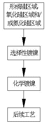
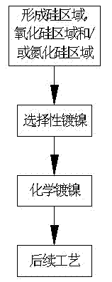
[0026] figure 1 It is a schematic flow sheet of a method for selectively growing nickel of the present invention; as figure 1 Shown, a kind of method of selective growth nickel of the present invention:

[0027] First, a silicon region consisting of a gate region and a source-drain region is prepared on a wafer, and a silicon oxide region and / or a silicon nitride region is prepared at the same time; wherein, at least one of the silicon oxide region and the silicon nitride region contains One; wherein the silicon oxide region includes sidewalls and shallow trench regions.

[0028] Then, immerse the wafer in a certain concentration of dilute hydrofluoric acid solution containing nickel ions to perform selective nickel plating to form a nickel seed layer on the silicon region; When in the solution for 5s to 600s, nickel ions will be deposited on t...


PUM


Abstract

The invention relates to the filed of semiconductor manufacturing, in particular to a method for selectively growing nickel. The nickel with required thickness is deposited in a silicon area by means of the method for selective nickel plating and no nickel is formed in a silicon oxide or silicon nitride area so as to guarantee that the nickel with required thickness is deposited in the silicon area and meanwhile damages such as organic contamination and the like cannot be caused.

Description

technical field [0001] The invention relates to the field of semiconductor integrated circuits and its manufacture, in particular to a method for selectively growing nickel. Background technique [0002] At present, with its excellent performance, electroless coating has won more and more people's trust, and its application scope also covers various fields of industrial production, although it has only gone a dozen years from early research to industrial application in China. Years away, but the speed of development is astonishing, and its potential development space is huge. [0003] The industrial application of electroless nickel plating mainly revolves around the following characteristics: [0004] 1. Throwing and deep plating capabilities, that is, for various geometric shapes, it is mainly used for surface plating of deep hole and blind hole workpieces. [0005] 2. Excellent anti-corrosion performance, that is, the chemical coating is amorphous, and it is mainly used...

Claims


Application Information

Patent Timeline
Patent Type & Authority Applications(China)
IPC IPC(8): C23C18/18C23C18/32
Inventor 周军傅昶
Owner SHANGHAI HUALI MICROELECTRONICS CORP
Why Eureka
Try Eureka