Film solar battery based on crystalline silicon and formation method thereof

A solar cell and thin-film technology, applied in circuits, photovoltaic power generation, electrical components, etc., can solve the problems of polluting the I-type amorphous silicon layer 13, reducing the bandgap width of thin-film solar cells, and reducing the photoelectric conversion efficiency of thin-film solar cells, etc. Achieve the effects of improving photoelectric conversion efficiency, reducing pollution, and increasing bandgap width

Inactive Publication Date: 2012-05-09
SILEVO CHINA
View PDF5 Cites 7 Cited by
  • Summary
  • Abstract
  • Description
  • Claims
  • Application Information

AI Technical Summary

Problems solved by technology

[0006] But there is following defect in above-mentioned technology: when the dopant ion concentration in P-type amorphous silicon layer 12 or N-type amorphous silicon layer 14 is higher, then P-type amorphous silicon layer 12 or N-type amorphous silicon layer 14 will Contaminate the I-type amorphous silicon layer 13, thereby reducing the photoelectric conversion efficiency of the thin-film solar cell; The bandgap width of the battery will also reduce the photoelectric conversion efficiency of thin-film solar cells

Method used


Image

  • Film solar battery based on crystalline silicon and formation method thereof
  • Film solar battery based on crystalline silicon and formation method thereof
  • Film solar battery based on crystalline silicon and formation method thereof

Examples


Embodiment 1

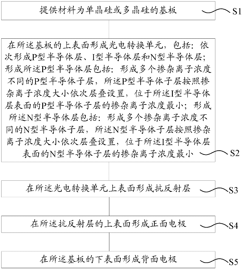
[0064] refer to figure 2 As shown, this embodiment provides a method for forming a thin-film solar cell based on crystalline silicon, including:

[0065] Step S1, providing a substrate made of monocrystalline silicon or polycrystalline silicon;

[0066] Step S2, forming a photoelectric conversion unit on the upper surface of the substrate, including: sequentially forming a P-type semiconductor layer, an I-type semiconductor layer, and an N-type semiconductor layer; forming the P-type semiconductor layer includes: forming a plurality of dopant ion concentration Different P-type semiconductor sub-layers, the P-type semiconductor sub-layers are sequentially stacked according to the doping ion concentration, and the P-type semiconductor sub-layer located on the surface of the I-type semiconductor layer has the smallest doping ion concentration; forming the N The N-type semiconductor layer includes: forming a plurality of N-type semiconductor sub-layers with different doping ion ...

Embodiment 2

[0118] This embodiment provides a method for forming a thin-film solar cell based on crystalline silicon, including:

[0119] The materials provided are monocrystalline silicon or polycrystalline silicon substrates;

[0120] An I-type semiconductor layer and a P-type semiconductor layer are sequentially formed on the substrate. The P-type semiconductor layer includes a plurality of P-type semiconductor sublayers with different dopant ion concentrations. The sizes are stacked in sequence, and the dopant ion concentration of the P-type semiconductor sub-layer located on the surface of the I-type semiconductor layer is the smallest.

[0121] Wherein, the substrate may be an N-type substrate.

[0122] Wherein, the steps of forming the I-type semiconductor layer and the P-type semiconductor layer are the same as those in Embodiment 1, and will not be repeated here. In this embodiment, the P-type semiconductor layer includes four P-type semiconductor sub-layers as an example.

[...

Embodiment 3

[0132] This embodiment provides a method for forming a thin-film solar cell based on crystalline silicon. The difference from Embodiment 2 is that in this embodiment, after forming the P-type semiconductor layer, an N-type semiconductor layer is also formed on the P-type semiconductor layer. .

[0133] Wherein, the dopant ion concentration in the N-type semiconductor layer may be evenly distributed, or may include multiple N-type semiconductor sub-layers with different dopant ion concentrations, which does not limit the protection scope of the present invention.

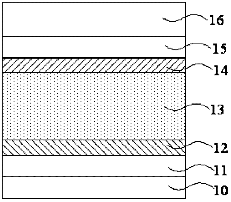
[0134] Specifically, refer to Figure 10 As shown, the thin-film solar cells based on crystalline silicon formed by the method of this embodiment include:

[0135] Substrate 30;

[0136] The I-type semiconductor layer 31, the P-type semiconductor layer 32, the N-type semiconductor layer 33, the anti-reflection layer 34 and the front electrode 35 which are located above the substrate 30 in turn; the P-type semicondu...


PUM


Abstract

The invention relates to a film solar battery based on crystalline silicon and a formation method thereof. The battery comprises a baseplate made of monocrystalline silicon or polysilicon, a photoelectric conversion unit positioned on the upper surface of the baseplate, an antireflection layer, a front electrode and a back electrode, wherein the photoelectric conversion unit successively comprises a P-type semiconductor layer, an I-type semiconductor layer and an N-type semiconductor layer,; the P-type semiconductor layer comprises multiple P-type semiconductor sublayers with different doped ion concentrations, and the P-type semiconductor sublayers are successively arranged in a stacking manner according to the doped ion concentrations; the N-type semiconductor layer comprises multiple N-type semiconductor sublayers with different doped ion concentrations, and the N-type semiconductor sublayers are successively arranged in a stacking manner according to the doped ion concentrations; the doped ion concentrations of the P-type semiconductor sublayer and the N-type semiconductor sublayer which are positioned on the surface of the I-type semiconductor layer are minimal; and the antireflection layer is positioned on the upper surface of the photoelectric conversion unit, the front electrode is positioned on the upper surface of the antireflection layer, and the back electrode is positioned on the lower surface of the baseplate. According to the invention, the photoelectric conversion efficiency can be improved.

Description

technical field [0001] The invention relates to the technical field of thin-film solar cells, in particular to a thin-film solar cell based on crystalline silicon and a forming method thereof. Background technique [0002] Thin-film solar cells are solar cells formed by depositing very thin (several micrometers to tens of micrometers) photoelectric materials on substrates such as glass, metal or plastic. Thin-film solar cells have a series of advantages such as power generation under weak light conditions, low energy consumption in the production process, and can greatly reduce raw material and manufacturing costs. They have become a research hotspot in recent years, and their market development potential is huge. [0003] Basic thin film solar cell structure, including single P-N junction, P-I-N / N-I-P and multi-junction. A typical single-junction P-N structure includes a P-type doped layer and an N-type doped layer. Single-junction P-N junction solar cells have two struct...

Claims


Application Information

Patent Timeline
Patent Type & Authority Applications(China)
IPC IPC(8): H01L31/0352H01L31/077H01L31/20
CPCY02E10/50Y02E10/547Y02P70/50
Inventor 傅建明杨瑞鹏
Owner SILEVO CHINA
Why Eureka
Try Eureka