Dual graphing method

A dual patterning and patterning technology, which is applied in the direction of photoplate making process, optics, and optomechanical equipment on the pattern surface, can solve the problem of low patterning precision, improve integration, improve precision, and reduce pattern lines. wide effect

Active Publication Date: 2012-05-30
SEMICONDUCTOR MANUFACTURING INTERNATIONAL (BEIJING) CORP
View PDF8 Cites 10 Cited by
  • Summary
  • Abstract
  • Description
  • Claims
  • Application Information

AI Technical Summary

Problems solved by technology

[0011] The problem solved by the invention is the problem of low patterning precision, so as to reduce the line width of the pattern and improve the integration degree of the device

Method used


Image

  • Dual graphing method
  • Dual graphing method
  • Dual graphing method

Examples


Embodiment Construction

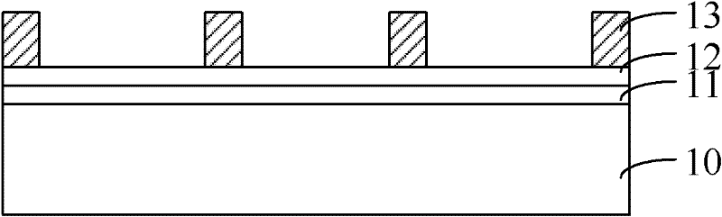
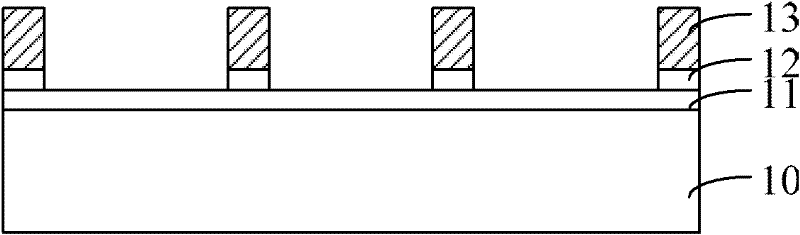
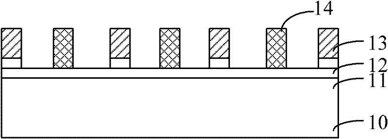
[0036] The double patterning method of the prior art divides the exposure pattern into two independent patterns with low density, and then exposes them separately. Due to the limitation of the exposure process, the patterning accuracy is still low, which cannot meet the needs of further processes.

[0037] In the double patterning method of the technical solution, the hard mask layer is first imprinted using an imprint mold, the first pattern is transferred to the hard mask layer, and then photoresist is formed on the hard mask layer layer, and pattern the photoresist layer, define a second pattern on the second photoresist, then use the patterned photoresist layer as a mask to etch the hard mask layer, and The second pattern is transferred to the hard mask layer. Using an imprinting mold for imprinting can get rid of the limitation of exposure process during lithography, which is beneficial to improve the precision of patterning, reduce the line width of patterns, and improve...


PUM


Abstract

The invention relates to a dual graphing method. The method comprises the following steps: 1, respectively providing a substrate and a stamping die, wherein a hard mask layer is formed on the substrate, the stamping die has a first graph, and the material of the hard mask is a metal or a metal compound; 2, stamping the hard mask layer by the stamping die to transfer the first graph to the hard mask layer; 3, forming a photoresist layer to cover the stamped hard mask layer; 4, graphing the photoresist layer to define a second graph; and 5, etching the hard mask layer with the graphed photoresist layer as a mask layer to transfer the second graph to the hard mask layer. The method is in favor of improving the graphing precision, reducing the graph line width and improving the device integration level.

Description

technical field [0001] The invention relates to semiconductor manufacturing technology, in particular to a double patterning method. Background technique [0002] Semiconductor technology continues to move towards smaller process nodes driven by Moore's Law. With the continuous advancement of semiconductor technology, the functions of devices are becoming more and more powerful, but the difficulty of semiconductor manufacturing is also increasing day by day. The lithography technology is the most critical production technology in the semiconductor manufacturing process. As the semiconductor process node enters 65 nanometers, 45 nanometers, and even lower 32 nanometers, the existing 193nm ArF light source lithography technology can no longer meet the needs of semiconductor manufacturing. Extreme ultraviolet lithography (EUV), multi-beam maskless technology and nanoimprint technology have become the research hotspots of next-generation lithography candidate technologies. How...

Claims


Application Information

Patent Timeline
Patent Type & Authority Applications(China)
IPC IPC(8): G03F7/00G03F1/00H01L21/02H01L21/311
Inventor 李凡张海洋
Owner SEMICONDUCTOR MANUFACTURING INTERNATIONAL (BEIJING) CORP
Why Eureka
Try Eureka