Chip reflow method of semiconductor manufacturing process

A manufacturing process and semiconductor technology, applied in semiconductor/solid-state device manufacturing, electrical components, circuits, etc., can solve the problems of low withstand voltage, large influence of device parameters, and inability to increase the withstand voltage value of the chip, so as to improve the withstand voltage of the chip. Value, technologically simple and feasible effect

Inactive Publication Date: 2012-05-30
PEKING UNIV FOUNDER GRP CO LTD +1
View PDF3 Cites 0 Cited by
  • Summary
  • Abstract
  • Description
  • Claims
  • Application Information

AI Technical Summary

Problems solved by technology

[0007] The above two methods have some unavoidable disadvantages. The first method has a greater impact on device parameters, while the second method only

Method used


Image

  • Chip reflow method of semiconductor manufacturing process
  • Chip reflow method of semiconductor manufacturing process
  • Chip reflow method of semiconductor manufacturing process

Examples


Embodiment Construction

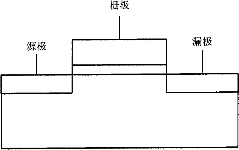
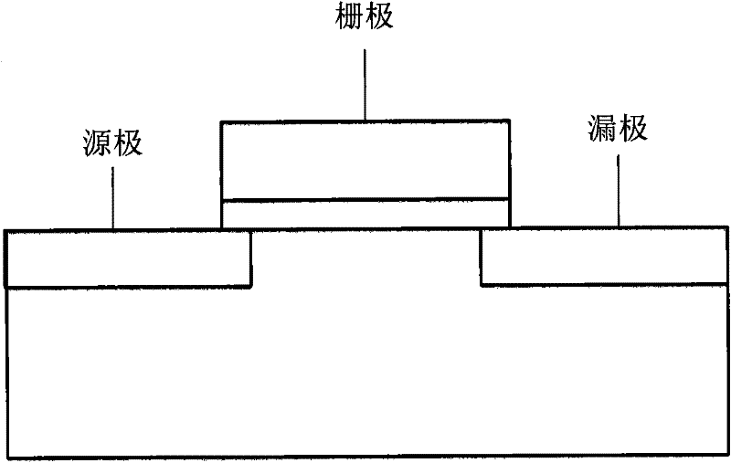
[0025] During the invention process, the inventor found that in the semiconductor manufacturing process flow, the higher the temperature in the reflow process, the more the lateral diffusion of the source and drain, resulting in a lower chip withstand voltage value. see Figure 1A ~ Figure 1B , Figure 1A A schematic diagram showing the structure of the source and drain before reflow, Figure 1B A schematic diagram of the structure after lateral diffusion of source and drain after reflow.

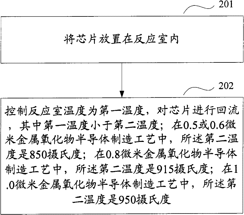
[0026] The invention provides a chip reflow method in a semiconductor manufacturing process. By changing the reflow temperature, the lateral diffusion of source and drain is reduced, and the purpose of improving the withstand voltage value of the entire chip is achieved. At the same time, the process is simple and feasible, and no additional process steps are added.

[0027] The solution of the present invention will be described in detail below in conjunction with the accompanying drawin...


PUM


Abstract

The embodiment of the invention discloses a chip reflow method of the semiconductor manufacturing process. The method comprises the following steps: placing a chip in a reaction chamber; and controlling the temperature of the reaction chamber to the first temperature, and reflowing the chip, wherein the first temperature is lower than the second temperature; in the manufacturing process of 0.5 or 0.6 micron of metal oxide semiconductors, the second temperature is 850 DEG C; in the manufacturing process of 0.8 micron of metal oxide semiconductors, the second temperature is 915 DEG C; and in the manufacturing process of 1.0 micron of metal oxide semiconductors, the second temperature is 950 DEG C. By adopting the embodiment of the invention, the permissible voltage of the whole chip can be increased.

Description


Claims


Application Information

Patent Timeline
Owner PEKING UNIV FOUNDER GRP CO LTD
Why Eureka
Try Eureka