Manufacturing method of transistor

A fabrication method and transistor technology, applied in semiconductor/solid-state device manufacturing, electrical components, circuits, etc., can solve problems such as device performance instability, and achieve the effects of improving stability, complete surface structure, and reducing leakage current

Active Publication Date: 2015-03-11
SEMICONDUCTOR MANUFACTURING INTERNATIONAL (BEIJING) CORP
View PDF4 Cites 0 Cited by
  • Summary
  • Abstract
  • Description
  • Claims
  • Application Information

AI Technical Summary

Problems solved by technology

[0011] In practice, it is found that the transistors made by the existing method have leakage current, and the performance of the device is unstable

Method used


Image

  • Manufacturing method of transistor
  • Manufacturing method of transistor
  • Manufacturing method of transistor

Examples


Embodiment Construction

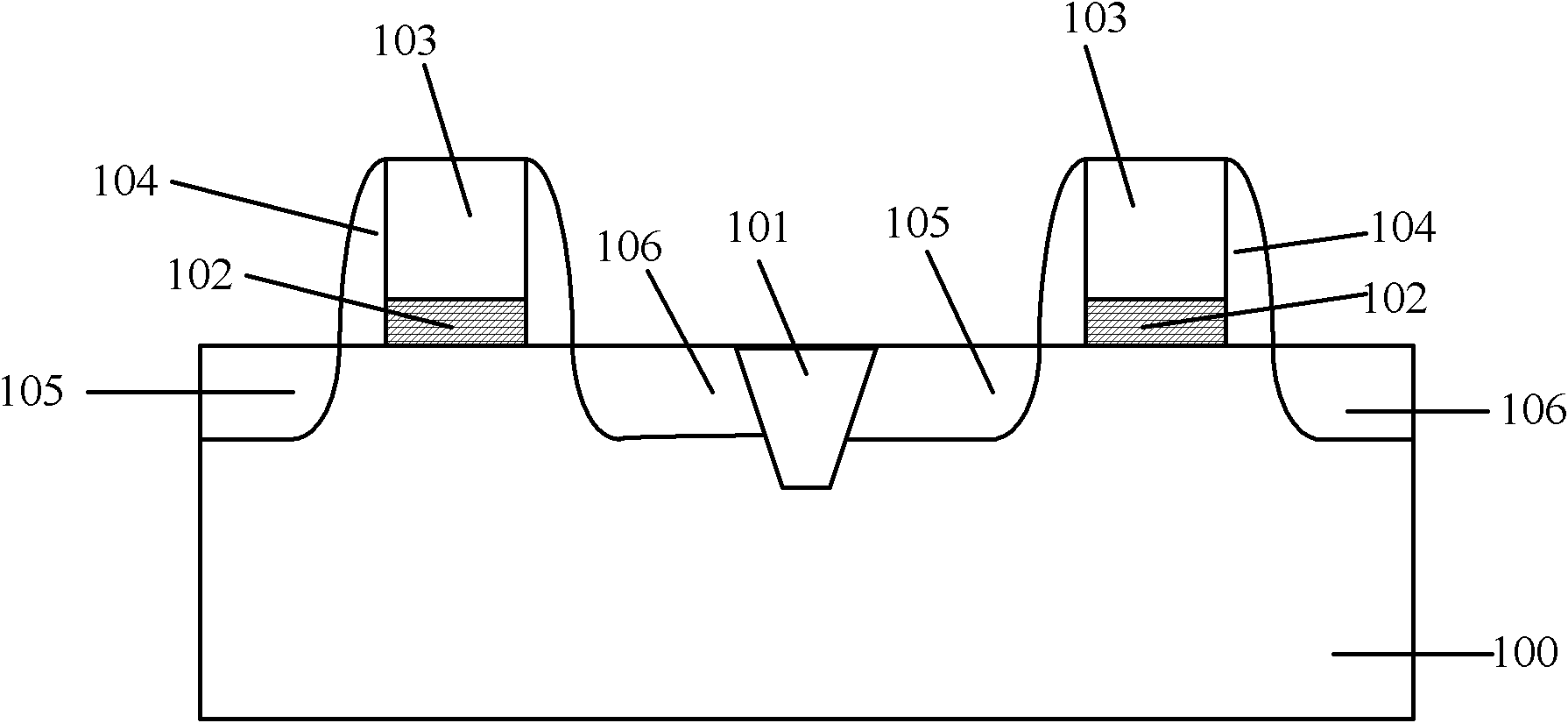
[0042] The transistor produced by the existing method has leakage current, and the performance of the device is unstable. After research by the inventors, it is found that the above problems are caused by the poor adhesion of the high-K dielectric layer to the gate dielectric layer and the sidewalls. Specifically, combine image 3 , during the process of removing the dummy gate 103, the gate dielectric layer 102 and the spacer 104 are damaged, so that the formed high-K dielectric layer 108 ( Figure 4 ) has poor adhesion to the sidewall 102 and the gate dielectric layer 108, which causes the leakage current of the transistor, thereby affecting the performance of the device.

[0043] In order to solve the above problems, the inventor proposes a method for making a transistor, please refer to Figure 6 The schematic flow chart of the transistor manufacturing method of the present invention shown, the method includes:

[0044] Step S1, providing a semiconductor substrate, a sa...


PUM


Abstract

The invention provides a manufacturing method of a transistor. The method comprises the following steps: providing a semiconductor substrate which is formed with a sacrificial layer and a dummy grid in order, wherein, spacers are formed on the semiconductor substrate at two sides of the sacrificial layer and the dummy grid; forming a source region and a drain region in the semiconductor substrate at the two sides of the dummy grid and the spacers; forming an interlayer dielectric layer which is level with the dummy grid on the semiconductor substrate; removing the dummy grid and the sacrificial layer, and forming a groove which is exposed from the semiconductor substrate; forming a gate dielectric layer at a bottom of the groove; forming a high-K dielectric layer on a sidewall of the groove and the gate dielectric layer respectively; forming a metal grid on the high-K dielectric layer in the groove, wherein, the metal grid is level with the interlayer dielectric layer. The gate dielectric layer of the present invention has a complete structure, adhesiveness between the high-K dielectric layer and the gate dielectric layer is raised, leakage current of the transistor is reduced, and stability of the transistor is improved.

Description

technical field [0001] The invention relates to the technical field of semiconductors, in particular to a method for manufacturing transistors. Background technique [0002] As the feature size of integrated circuits shrinks to the deep submicron field, the gate size of transistors shrinks, and the thickness of the silicon dioxide layer as the gate dielectric layer also needs to be reduced accordingly to increase the gate capacitance of transistors and prevent devices from appearing. short channel effect. However, when the thickness of the gate dielectric layer is gradually reduced, and the thickness of the gate dielectric layer is reduced to less than 3 nanometers, many problems will arise, such as: (1) leakage current increases; (2) impurity diffusion, that is, the gate dielectric layer and the semiconductor substrate There is an impurity concentration gradient between them, and the impurity will diffuse from the gate into the semiconductor substrate or be fixed in the ga...

Claims


Application Information

Patent Timeline
Patent Type & Authority Patents(China)
IPC IPC(8): H01L21/336H01L21/311H01L21/283H01L21/8234
Inventor 康芸李敏
Owner SEMICONDUCTOR MANUFACTURING INTERNATIONAL (BEIJING) CORP
Why Eureka
Try Eureka