High-efficiency high-voltage vertical through hole bonding type light emitting diode (LED) chip and manufacture method thereof

An LED chip and vertical through-hole technology, applied in electrical components, electrical solid devices, circuits, etc., can solve the problems of long-term use of high-power LEDs, cumbersome processes, differences in thermal expansion coefficients, etc., to reduce the number of packaging wires, increase Light-emitting area and efficiency, the effect of improving light-emitting efficiency

Inactive Publication Date: 2012-05-30
上海蓝宝光电材料有限公司
View PDF0 Cites 3 Cited by
  • Summary
  • Abstract
  • Description
  • Claims
  • Application Information

AI Technical Summary

Problems solved by technology

However, compared with traditional horizontal LEDs, the process of vertical LEDs is cumbersome, and the difference in thermal expansion coefficient and adhesion between the LED chip after removing the sapphire and the substrate after reposting is a hidden danger for the long-term use of high-power LEDs in the future.

Method used


Image

  • High-efficiency high-voltage vertical through hole bonding type light emitting diode (LED) chip and manufacture method thereof
  • High-efficiency high-voltage vertical through hole bonding type light emitting diode (LED) chip and manufacture method thereof
  • High-efficiency high-voltage vertical through hole bonding type light emitting diode (LED) chip and manufacture method thereof

Examples


Embodiment Construction

[0023] DETAILED DESCRIPTION OF THE PREFERRED EMBODIMENTS Specific embodiments of the present invention will be described below with reference to the accompanying drawings.

[0024] Making the structure of the LED chip according to the first embodiment of the present invention comprises the following steps:

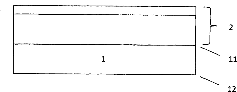
[0025] figure 1 It is a light emitting epitaxial layer 2 formed on the substrate 1 and its first surface 11 of the LED chip according to the first embodiment of the present invention. The light emitting epitaxial layer is a light emitting structure for LED well known to those skilled in the art, such as group IIIV Compound semiconductor light-emitting structures, etc. The emitted light includes light propagating away from the substrate and light propagating toward the substrate 1 , and the light propagating toward the substrate at least partially passes through the substrate 1 .

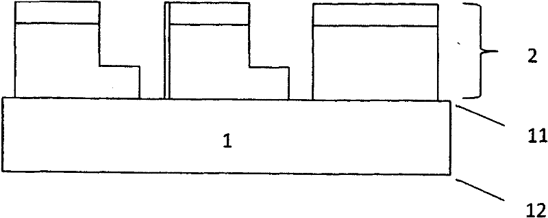
[0026] figure 2 It shows that the LED chip according to the first embodiment of the prese...


PUM


Abstract

The invention provides a structure and a method for manufacturing a high-efficiency high-voltage vertical through hole bonding type light emitting diode (LED) chip. The structure comprises at least one chip and a bottom plate, wherein the chip comprises a substrate and a luminous epitaxial layer grown on the substrate surface, the substrate is provided with a first surface and a second surface opposite to the first surface, a reflecting layer is formed on the second surface of the substrate, a bottom plate with good heat radiation performance is bonded on the reflecting layer formed on the second surface of the substrate through wafers, and the luminous epitaxial layer is formed on the first surface, wherein light emitted by the luminous epitaxial layer comprises light spread in a direction far away from the substrate and light spread in a direction towards the substrate, the light spread in the direction towards the substrate is at least partially transmitted from the substrate and is then reflected by the reflecting layer, and at least one electrode of the luminous epitaxial layer is connected with the bottom plate through a through hole. The invention also provides the high-efficiency high-voltage vertical through hole bonding type LED chip manufactured by the method.

Description

technical field [0001] The invention relates to making a high-efficiency high-voltage vertical through-hole bonding type LED chip and a structure for making the high-efficiency high-voltage vertical through-hole bonding type LED chip. Background technique [0002] Compared with traditional DC LED lighting products, high-voltage LED products do not require transformers, which not only saves costs, but also has more stable performance, more uniform current density, and higher luminous efficiency. It is the development trend of LED core technology to pay equal attention to the improvement of luminous efficiency and the reduction of device cost. At present, the improvement of epitaxial chip technology has caused the cost ratio to drop rapidly, but the discrete chip back-end process and traditional packaging process have become cost bottlenecks. In addition, when the efficiency of the LED device is greater than 100lm / W, it is also faced with the problems of light output efficien...

Claims


Application Information

Patent Timeline
Patent Type & Authority Applications(China)
IPC IPC(8): H01L33/64H01L33/46H01L33/38H01L27/15H01L33/00
Inventor 钟伟荣蔡凤萍李刚
Owner 上海蓝宝光电材料有限公司
Why Eureka
Try Eureka