Vertical parasitic PNP device in BiCMOS (Bipolar Complementary Metal-Oxide-Semiconductor) process and preparation method thereof

A technology with vertical parasitics and process conditions, applied in the direction of semiconductor/solid-state device manufacturing, semiconductor devices, electrical components, etc., can solve the problems of large device area, reduced device size, large collector connection resistance, etc., to achieve high current amplification factor, The effect of improving current gain and reducing area

Active Publication Date: 2012-06-06
SHANGHAI HUAHONG GRACE SEMICON MFG CORP
View PDF5 Cites 12 Cited by
  • Summary
  • Abstract
  • Description
  • Claims
  • Application Information

AI Technical Summary

Problems solved by technology

The disadvantage is that the device area is large and the connection resistance of the collector is large
Since the extraction of the collector electrode in the prior art is realized through another active region adjacent to the collector region, and the other active region and the collector region need to be isolated by STI or other field oxygen, such This greatly limits the further reduction of the device size

Method used


Image

  • Vertical parasitic PNP device in BiCMOS (Bipolar Complementary Metal-Oxide-Semiconductor) process and preparation method thereof
  • Vertical parasitic PNP device in BiCMOS (Bipolar Complementary Metal-Oxide-Semiconductor) process and preparation method thereof
  • Vertical parasitic PNP device in BiCMOS (Bipolar Complementary Metal-Oxide-Semiconductor) process and preparation method thereof

Examples


Embodiment B

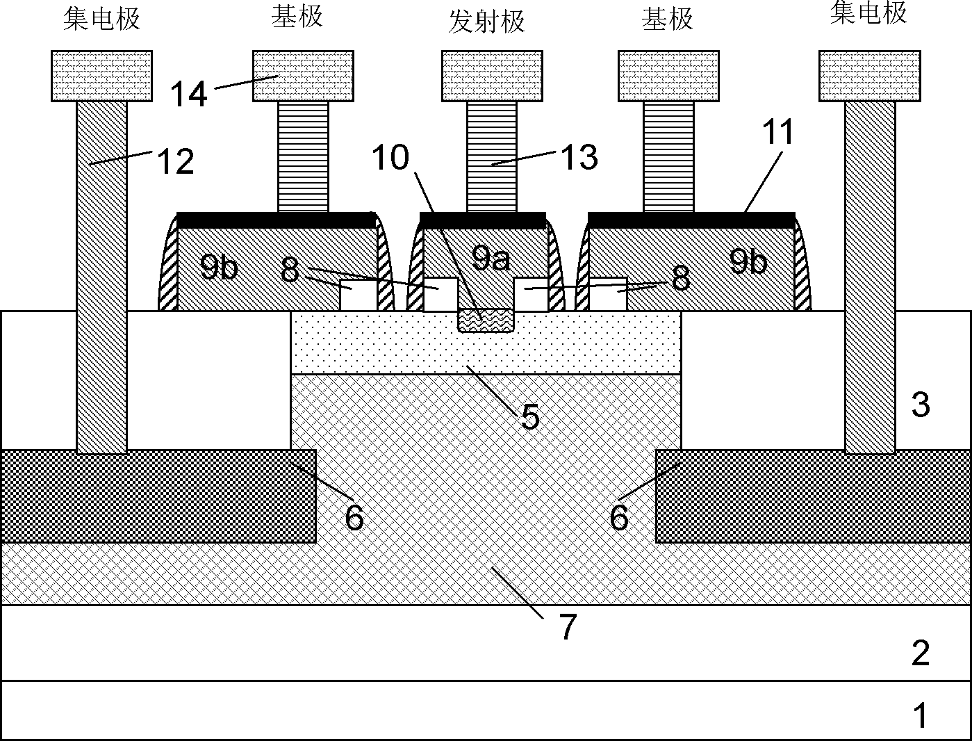
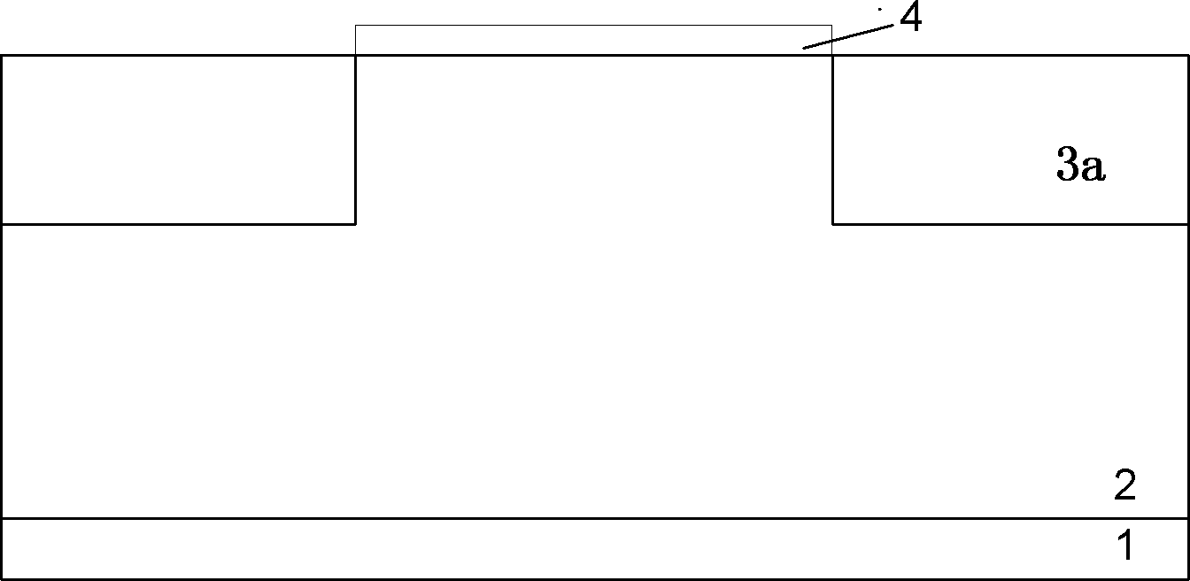
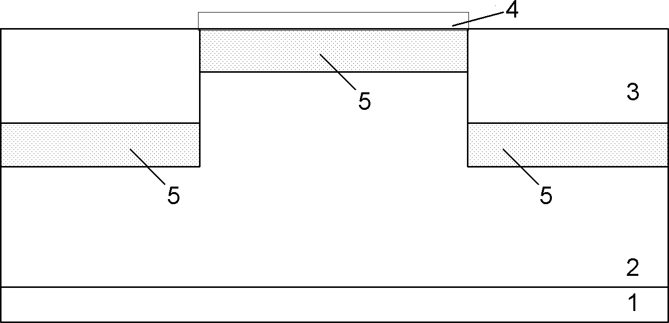
[0041] Such as figure 1 Shown is a schematic structural view of the vertical parasitic PNP device in the BiCMOS process of the embodiment of the present invention. The vertical parasitic PNP device in the BiCMOS process of the embodiment of the present invention is formed on a P-type silicon substrate 1 and placed on the P-type silicon substrate 1. An N-type deep well 2 is formed on a silicon substrate 1, and the active region is isolated by a shallow trench field oxygen 3, which is shallow trench isolation (STI). The vertical parasitic PNP device includes:

[0042] A collector region 7 is composed of a P-type ion implantation region formed in the active region, and the depth of the collector region 7 is greater than or equal to the depth of the bottom of the shallow trench field oxygen 3 . The impurity implanted in the P-type ion implantation of the collector region 7 is boron, which is implemented in two steps: the implantation dose in the first step is 1e11cm -2 ~5e13cm -...


PUM


Abstract

The invention discloses a vertical parasitic PNP device in a BiCMOS (Bipolar Complementary Metal-Oxide-Semiconductor) process. The vertical parasitic PNP device comprises a collector region, a base region, an emitter region, a P type buried layer and N type polycrystalline silicon, wherein the buried layer is formed at a shallow trench filed oxide bottom surrounding the collector region and is in contact with the collector region through a deep hole formed at the top of the buried layer to lead out a collector electrode; the N type polycrystalline silicon is formed at the upper part of the base region and is used for leading out a base electrode; and the emitter region is composed of a P type shallow junction formed in the base region and P type polycrystalline silicon arranged above the base region. The invention also discloses a preparation method of the vertical parasitic PNP device in the BiCMOS process. The device disclosed by the invention can serve as an output device in a high-speed high-gain BiCMOS circuit, and therefore another device choice is provided for the circuit. According to the invention, the area of the device can be reduced effectively, the resistance of the collector electrode of a PNP transistor can be lowered, the frequency performance of the device can be improved and the gain of the device can be enhanced. No extra process condition is required in the preparation method disclosed by the invention, thereby reducing the production cost.

Description

technical field [0001] The invention relates to the field of semiconductor integrated circuit manufacturing, in particular to a vertical parasitic PNP device in a BiCMOS process, and also relates to a method for manufacturing the vertical parasitic PNP device in the BiCMOS process. Background technique [0002] In RF applications, higher and higher device characteristic frequencies are required. In BiCMOS process technology, NPN transistors, especially germanium-silicon heterojunction transistors (SiGe HBT) or germanium-silicon-carbon heterojunction transistors (SiGeC HBT) are good choices for UHF devices. And the SiGe process is basically compatible with the silicon process, so SiGe HBT has become one of the mainstreams of UHF devices. In this context, the requirements for the output device are correspondingly increased, such as having a current gain coefficient and a cutoff frequency not less than 15. [0003] In the prior art, the output device can adopt a vertical para...

Claims


Application Information

Patent Timeline
Patent Type & Authority Applications(China)
IPC IPC(8): H01L29/732H01L29/06H01L21/331H01L29/43H01L21/60
Inventor 刘冬华董金珠
Owner SHANGHAI HUAHONG GRACE SEMICON MFG CORP
Why Eureka
Try Eureka