Resistance random access memory with cross array structure and preparation method

A technology of resistive memory and interleaved array, which is used in static memory, digital memory information, information storage and other directions

Inactive Publication Date: 2012-06-27
PEKING UNIV
View PDF4 Cites 14 Cited by
  • Summary
  • Abstract
  • Description
  • Claims
  • Application Information

AI Technical Summary

Problems solved by technology

[0005] The technical problem to be solved by the present invention is: how to provide a resistive

Method used


Image

  • Resistance random access memory with cross array structure and preparation method
  • Resistance random access memory with cross array structure and preparation method
  • Resistance random access memory with cross array structure and preparation method

Examples


Embodiment Construction

[0035] The specific implementation manners of the present invention will be further described in detail below in conjunction with the accompanying drawings and embodiments. The following examples are used to illustrate the present invention, but are not intended to limit the scope of the present invention.

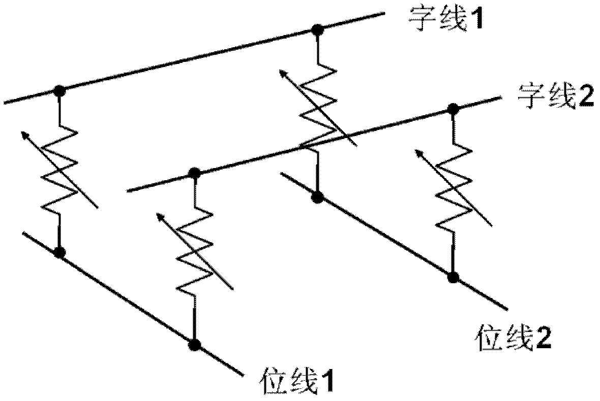
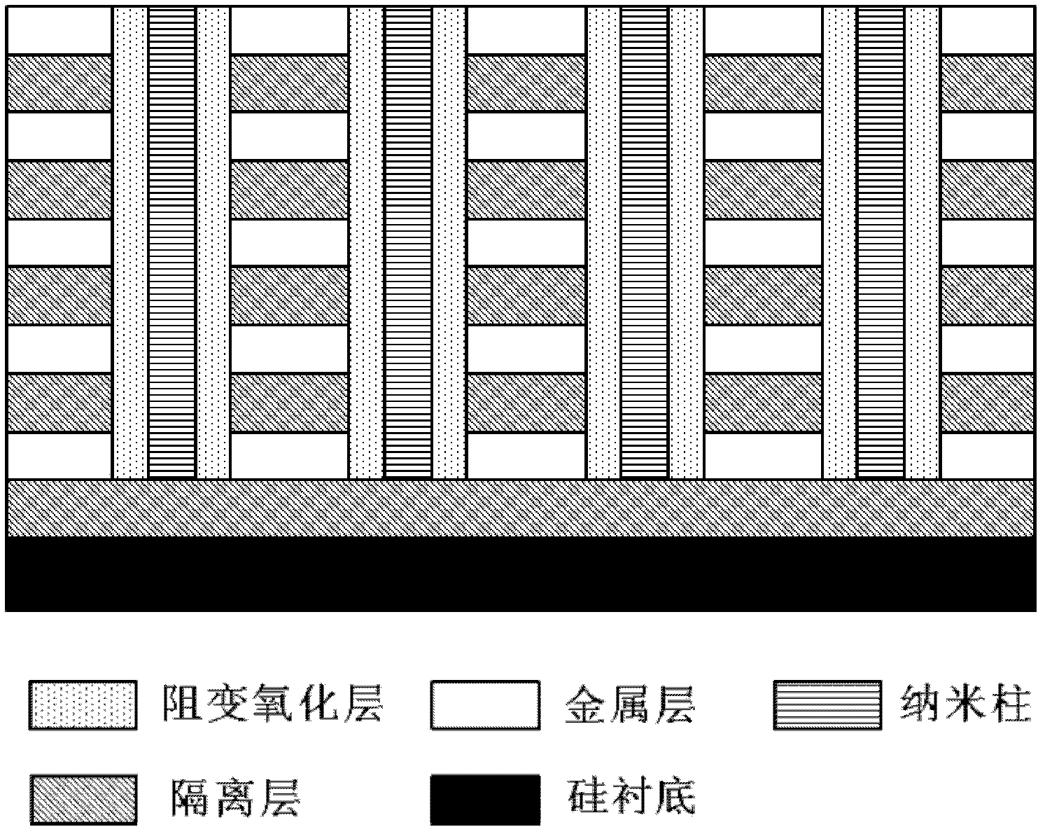
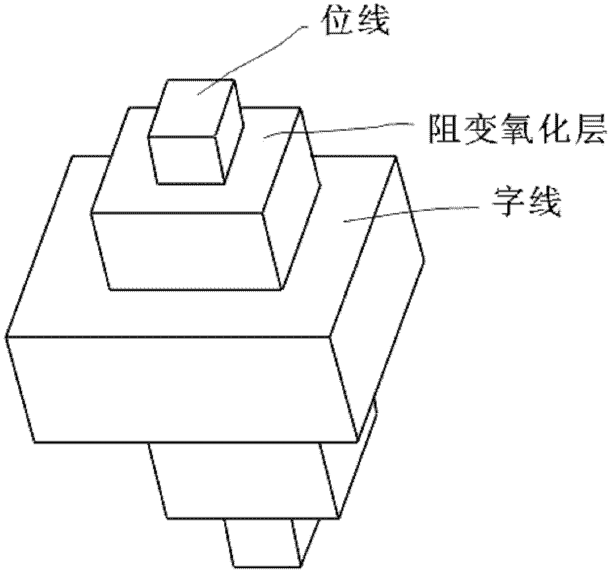
[0036] The structure of the memory of the present invention is described below by setting 5 layers of metal layers and isolation layers at intervals. In the actual structure, more layers can be repeated, so the protection scope of the present invention is not limited. Refer to figure 2 , the memory of this embodiment includes: a silicon substrate, a first isolation layer is provided on the silicon substrate, at least one nano-column perpendicular to it is provided on the first isolation layer, and the nano-column around the nano-column The side wall is provided with a resistive oxide layer around the outer wall of the resistive oxide layer, and a metal layer and a second ...


PUM

PropertyMeasurementUnit
Thicknessaaaaaaaaaa
Thicknessaaaaaaaaaa
Thicknessaaaaaaaaaa

Abstract

The invention discloses a resistance random access memory with a cross array structure and a preparation method and relates to the technical field of a semiconductor integrated circuit and manufacturing thereof. The memory comprises a silicon substrate. A first isolation layer is arranged on the silicon substrate. At least one nano column vertical to the first isolation layer is arranged on the first isolation layer. A resistive oxide layer is arranged around the side wall of the nano column by a circle. A metal layer and a second isolation layer are arranged around the outer side wall of the resistive oxide layer by a circle at intervals from bottom to top. The nano column is made of metal. According to a certain structure setting, the aim of providing the memory which is suitable for three-dimensional integration under the condition that the process complexity is not increased is fulfilled.

Description

technical field [0001] The invention relates to the technical field of semiconductor integrated circuits and their manufacture, in particular to a resistive variable memory with a cross-array structure and a preparation method thereof. Background technique [0002] Non-volatile memory has the advantage of maintaining data information when there is no power supply, and plays a very important role in the field of information storage. Among them, the new non-volatile memory using resistance change has the advantages of high speed (<1ns), low operating voltage (<1.5V), high storage density, multi-value storage on one unit, and easy integration. It is very promising to become Mainstream technology for next-generation semiconductor memory. This resistive variable memory (RRAM) generally has a metal-insulator-metal sandwich structure, that is, a layer of dielectric film material with resistive properties is added between two layers of metal electrodes, and these resistive ma...

Claims


Application Information

Patent Timeline
IPC IPC(8): H01L45/00H01L27/24G11C13/00
Inventor 高滨康晋锋刘力锋刘晓彦
Owner PEKING UNIV
Why Eureka
Try Eureka