Read-Only Cache Memory for Embedded Chips

An embedded chip and high-speed buffering technology, which is applied in the direction of memory systems, instruments, input/output to record carriers, etc., can solve the problems of inconvenient user configuration, increased cache memory (CACHE complexity, increased chip area and power consumption, etc.) , to achieve the effect of improving performance and practicability, replacing efficiency and resource overhead balance, and reducing module power consumption

Active Publication Date: 2014-10-22
苏州国芯科技股份有限公司
View PDF3 Cites 2 Cited by
  • Summary
  • Abstract
  • Description
  • Claims
  • Application Information

AI Technical Summary

Problems solved by technology

If the traditional cache memory (CACHE) that can be cached for both read and write operations is used, its redundant write operation cache control will greatly increase the complexity of the cache memory (CACHE), which not only increases the area and power consumption of the chip, And it will bring a lot of inconvenience to the user's configuration

Method used


Image

  • Read-Only Cache Memory for Embedded Chips
  • Read-Only Cache Memory for Embedded Chips
  • Read-Only Cache Memory for Embedded Chips

Examples


Embodiment

[0034] Embodiment: A kind of read-only cache memory applied to embedded chip

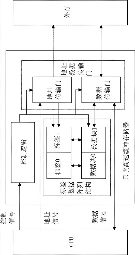
[0035] like figure 1 As shown, the read-only cache memory is composed of three parts: tag data array structure, control logic module, and address data transmission gate. The three parts are described below:

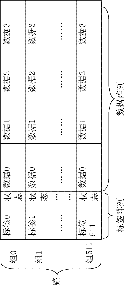
[0036] 1. Tag data array structure

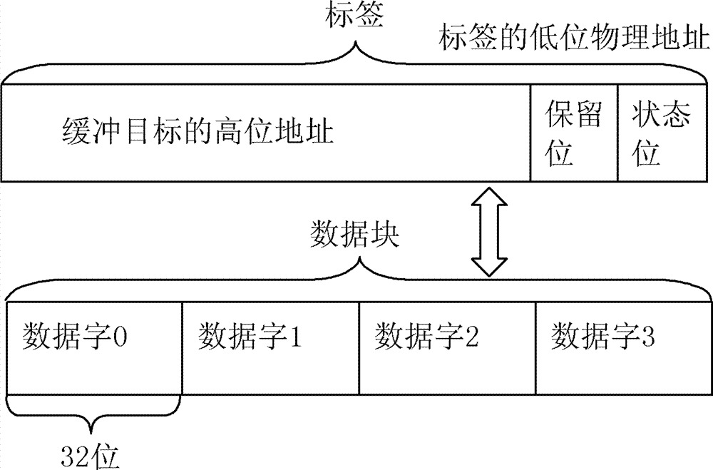
[0037] like figure 2 and image 3 As shown, the tag data array structure refers to the tag data array structure defined on the SRAM memory bank for read-only buffering. The tag data array structure is composed of at least two tag data arrays, each tag data array is composed of several groups of tag data, and each group of tag data is composed of tags and data blocks. figure 2 Only draw a schematic diagram of the label data array of a certain road (other roads are basically the same as the schematic diagram of this road), where group 0, group 1 and group 511 represent groups, group 0 is composed of label 0 and data blocks, and data blocks are composed of...


PUM


Abstract

The invention provides a read-only cache memory applying on embedded chips and has the innovation that the read-only cache memory mainly consists of a label data array structure, a control logic and an address data transmission gate. The invention relates to a design scheme of the read-only cache memory applying on the embedded chips, according to the scheme, the resource configuration is carried out in a group association address mapping way; an interface is provided between a chip processor and an external memory which only needs read operation cache; and label and data replacing management is carried out by adopting an improved polling algorithm. The scheme ensures the performance of the cache memory and acts according to actual conditions to optimize the module structure effectively, therefore, the module area is increased, the module energy consumption is reduced, and the utilization rate of the space of the cache memory is improved.

Description

technical field [0001] The invention relates to a cache memory, in particular to a read-only cache memory applied to an embedded chip, and belongs to the technical field of high-speed memory management. The so-called embedded chip refers to the chip where the microprocessor in the embedded system is located. Background technique [0002] With the continuous improvement of embedded chip design level and manufacturing process, the processing speed of the on-chip processor is also continuously improved. However, due to its own structure and operating mechanism, the response speed of the external memory is far lower than that of the processor. This imbalance in speed is increasingly becoming the bottleneck that restricts the overall processing speed of embedded chips. In order to deal with this problem, cache memory (CACHE), whose response speed is equivalent to that of the processor, is also gradually integrated into the embedded chip. On the one hand, this technology has be...

Claims


Application Information

Patent Timeline
Patent Type & Authority Patents(China)
IPC IPC(8): G06F12/08G06F3/06G06F12/121
CPCY02B60/1225Y02D10/00
Inventor 郑茳肖佐楠匡启和林雄鑫吴凯祺
Owner 苏州国芯科技股份有限公司
Why Eureka
Try Eureka