Device for removing display pixel particle effect and OLED (organic light emitting diode) display screen

A technology for displaying pixels and particle effects, applied in identification devices, static indicators, optics, etc., can solve problems such as particle effects, achieve soft light, better visual enjoyment, and improve the pixel filling rate

Active Publication Date: 2015-04-08
GUANGDONG VTRON TECH CO LTD
View PDF8 Cites 1 Cited by
  • Summary
  • Abstract
  • Description
  • Claims
  • Application Information

AI Technical Summary

Problems solved by technology

[0005] The purpose of the present invention is to provide a device and OLED display screen for eliminating the grain effect of display pixels, so as to solve the problem of grain effect caused by the gap between display pixel groups

Method used


Image

  • Device for removing display pixel particle effect and OLED (organic light emitting diode) display screen
  • Device for removing display pixel particle effect and OLED (organic light emitting diode) display screen
  • Device for removing display pixel particle effect and OLED (organic light emitting diode) display screen

Examples


Embodiment 1

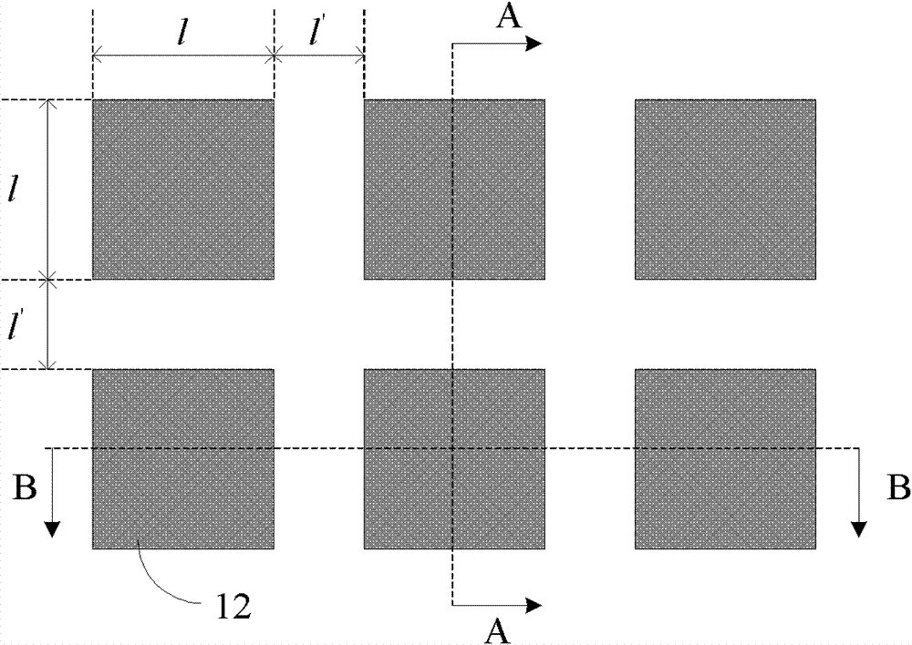
[0030] The optical lens device 01 includes an array of plano-convex lenses 011 respectively covering all the display pixel groups 12 in front of the OLED display screen, see Figure 4 As shown, Figure 4 Is a three-dimensional view of the plano-convex lens 011. The bottom surface of the plano-convex lens 011 is square, the side length is L, and the edge thickness is H, where L=1+l', l is the effective light-emitting area of ​​the display pixel group 12, and l'is the phase The spacing between adjacent display pixels. The center of the bottom surface of each plano-convex lens 011 corresponds to the center of the display pixel group 12, see Figure 5 As shown, each dashed box in the figure corresponds to a plano-convex lens 011, and the plano-convex lens 011 array corresponding to all the display pixel groups 12 constitutes the entire optical device.

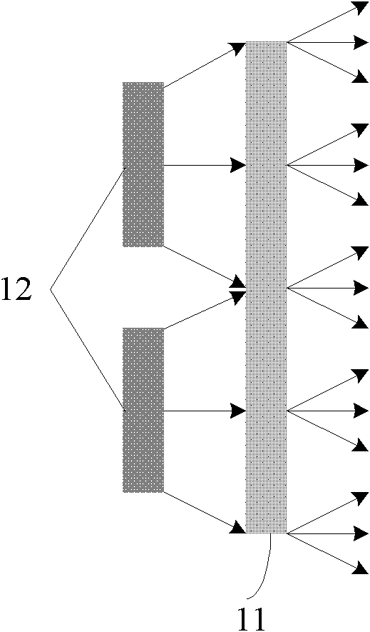
[0031] See Image 6 As shown, Image 6 Yes Figure 5 The AA cross-sectional view in, shows the ab and cd of the pixel group 12. After...

Embodiment 2

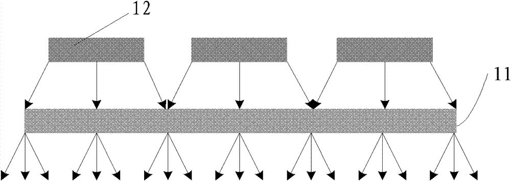
[0036] The optical mirror device 01 includes an array of optical microstructure light guide plates 012 respectively covering all the display pixel groups 12 in front of the OLED display screen; see Figure 7 As shown, the optical microstructure light guide plate 012 includes a light guide plate 0121 and a triangular prism 0122. The bottom surface of the light guide plate 0121 is square. The center of the bottom surface of the light incident side corresponds to the center of the display pixel group 12, and the side length is l (that is, the display pixel group 12 The length of the side of the light-emitting area), on the light-emitting side of the light guide plate 0121, along the direction (the direction of the dotted line in the figure) between the center of the light guide plate 0121 and the four vertex corners, at least one row of triangular prisms 0122 are respectively arranged for The light of the display pixel group 12 is refracted to the surroundings, the side of the light...


PUM


Abstract

The invention provides a device11 for removing display pixel particle effect, which comprises an optical lens device 01 and a scattering device 02. The optical lens device 01 covers the front of a display pixel group 12 of an OLED (organic light emitting diode) display screen, the scattering device 02 is arranged in front of the optical lens device 01, and the optical lens device 01 is used for refracting light emitted from the display pixel group 12 to the surrounding. The invention further provides an OLED display screen, which comprises at least one OLED display module 13, a signal driving circuit 14, a power source 15, a fixing bar 16, a backing plate 17 and the device 11 for removing the display pixel particle effect. By the device for removing display pixel particle effect, the pixel fill rate is increased, the display pixel particle effect of the OLED display screen is removed, and excellent visual experience can be brought to viewers.

Description

Technical field [0001] The invention relates to a device for eliminating the particle effect of display pixels and an OLED display screen, belonging to the field of display technology. Background technique [0002] The OLED super-resolution display wall provides a unified information display platform, and currently has a wide range of applications in power, transportation, energy, telecommunications, military and public security, enterprises, radio and television, etc. [0003] OLED is a self-luminous material and does not need a backlight. At the same time, it has a wide viewing angle, uniform picture quality, fast response speed, easy colorization, and can achieve light emission with a simple driving circuit. The manufacturing process is simple and can be made into a flexible panel. The principle of light, thin, short and small, the application range belongs to small and medium-sized panels. Display aspect: active light emission, wide viewing angle range; fast response speed, st...

Claims


Application Information

Patent Timeline
Patent Type & Authority Patents(China)
IPC IPC(8): G09F9/33G09G3/32G02B27/10G09G3/3208
Inventor 刘伟俭孟凡华黄镇刘文军
Owner GUANGDONG VTRON TECH CO LTD
Why Eureka
Try Eureka