Chucking device and chucking method

A substrate card, vacuum suction technology, applied in workpiece clamping devices, electrical components, sleeve/socket connections, etc., can solve problems such as difficult control, small width, wafer distortion, etc., and achieve the effect of eliminating warpage

Inactive Publication Date: 2012-07-04
FUJI ELECTRIC CO LTD
View PDF15 Cites 8 Cited by
  • Summary
  • Abstract
  • Description
  • Claims
  • Application Information

AI Technical Summary

Problems solved by technology

[0007] In addition, with the pin-snap-type chucking device, there occurs a problem that, due to the sagging of the semiconductor substrate between the protrusions, the position of the contact point of the surface of the semiconductor substrate with each protrusion is different from that of placing the semiconductor substrate on the protrusions. More deviation than without vacuum suction (hereafter referred to as wafer distortion)
When the interval between adjacent protrusions is about 0.7 mm or less when anisotropic etching is used to form the protrusions of the quadrangular pyramid on the base, the width of the opening portion of the mask covering the non-etched area of ​​the base is too small, and Difficult to control the amount removed by etching along the crystal plane
For this reason, the controllability of the height of each protrusion and the interval between adjacent protrusions is lost

Method used


Image

  • Chucking device and chucking method
  • Chucking device and chucking method
  • Chucking device and chucking method

Examples


no. 1 example

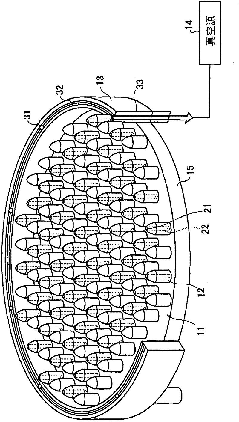
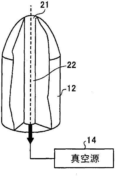
[0089] figure 1 is a view schematically showing the chucking device according to the first embodiment. also, figure 2 and 3 is schematically showing the structure figure 1 Views of the components of the snap-in device shown. figure 1 The shown suction device includes a base 11, a cylindrical peripheral portion 13, a plurality of suction holes 21 and 31, and a vacuum source 14, the base 11 is provided with a plurality of protrusions 12 supporting the central portion of the semiconductor substrate, and the cylindrical peripheral portion The portion 13 supports the outer peripheral portion of the semiconductor substrate, the plurality of suction holes 21 and 31 chuck the semiconductor substrate, and the vacuum source 14 vacuums the plurality of suction holes at different timings.

[0090] The base 11 has, for example, a circular planar shape. The diameter of the base 11 is slightly smaller than that of the semiconductor substrate. In addition, the base 11 may be compose...

no. 2 example

[0142] Figure 11 is a view showing a chucking method using a chucking device according to the second embodiment. In the first embodiment, it is possible to chuck a semiconductor substrate (hereinafter referred to as a ribbed wafer) 51 having a stepped form due to a peripheral portion 52 remaining thickly around the periphery.

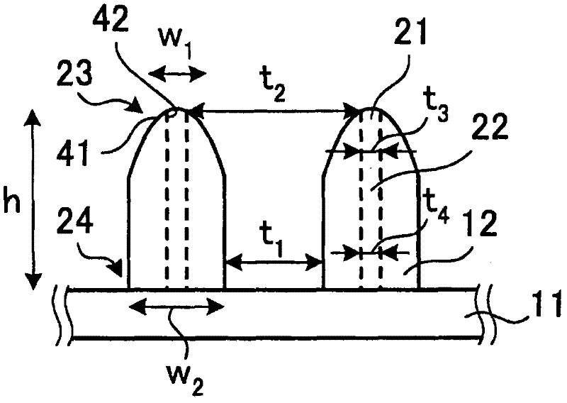
[0143] In the second embodiment, as Figure 11 As shown in FIG. and the second suction hole 31 provided in the peripheral portion 13 . In addition, the height h of the protruding portion 12 can be made higher than that of the outer peripheral portion 13, and the depressed portion of the ribbed wafer 51 which is thinner due to the outer peripheral portion 52 is only snapped to the first suction provided in the protruding portion 12. Holes 21 (not shown). In this case, the outer peripheral portion 52 of the ribbed wafer 51 can be snapped to the second suction holes 31 provided in the peripheral portion 13 . The structure of the sucking device and th...

no. 3 example

[0146] Figure 12 and 13 is a view showing a chucking method using the chucking device according to the third embodiment. In the first embodiment, the peripheral portion 53 may be provided so as to be able to be raised and lowered in the vertical direction with respect to the surface of the semiconductor substrate supported on the peripheral portion 53 .

[0147] A description is given of the chucking method of the third embodiment, taking, for example, the case of chucking the rear surface side of a semiconductor substrate that is concave and warped on the front surface side as an example. First, using a transfer arm (not shown) or the like, the semiconductor substrate 1 is placed with the rear surface downward on the peripheral portion 53 installed so as to be able to be raised and lowered above the base 11, as shown in FIG. Figure 12 shown. Next, a second step of snapping the outer peripheral portion of the rear surface of the semiconductor substrate 1 to the second suc...


PUM


Abstract

The invention provides a chucking device and chucking method that can prevent a foreign object being caught between the device and a semiconductor substrate and can hold the semiconductor substrate in a condition in which the semiconductor substrate flatness is maintained or increased. The chucking device includes plural protruding portions that support the central portion of a semiconductor substrate and that are provided on a base portion. The chucking device also includes a cylindrical peripheral portion that supports the outer peripheral portion of the semiconductor substrate, plural suction holes that chuck the semiconductor substrate, and a vacuum source that vacuum draws the plural suction holes at differing timings. A plurality of mutually independent vacuum drawable suction holes are provided in at least one portion of the protruding portions. The vacuum drawable suction holes are independently arranged in the peripheral portion. After the semiconductor substrate is arranged on the protruding portions and the peripheral portion, the suction holes are drawable by using the vacuum source and on the semiconductor substrate at differing timings.

Description

technical field [0001] The invention relates to a suction device and a suction method. Background technique [0002] In recent years, the importance of power semiconductor devices such as insulated gate bipolar transistors (IGBTs) or insulated gate field effect transistors (MOSFETs) has increased as environmentally friendly electronic devices. Chucking devices that hold semiconductor substrates by vacuum chucking have been proposed for transferring semiconductor substrates along a production line or for fixing semiconductor substrates to support racks in manufacturing steps of semiconductor devices. [0003] Figure 20 is a diagram showing hitherto known snapping devices. Figure 20 The snap-in shown in includes a base 101 in which an annular or radial groove portion 102 is provided. Vent holes (vacuum system) 103 and 104 coupled to the groove portion 102 are vacuumed, whereby the vacuum vacuum chucks the semiconductor substrate 1 onto the base 101 (see, for example, U.S. P...

Claims


Application Information

Patent Timeline
Patent Type & Authority Applications(China)
IPC IPC(8): H01L21/683B25B11/00
CPCH01L21/6838B25B11/005H01L21/6875Y10T29/49998Y10T29/53191Y10T279/11
Inventor 大井浩之
Owner FUJI ELECTRIC CO LTD
Why Eureka
Try Eureka