Preparation method and device of LED epitaxial wafer

A technology for LED epitaxial wafers and preparation devices, applied in electrical components, circuits, semiconductor devices, etc., can solve problems such as waste of materials, expensive equipment, and increased production costs.

Inactive Publication Date: 2011-05-25
SUZHOU INST OF NANO TECH & NANO BIONICS CHINESE ACEDEMY OF SCI
View PDF5 Cites 8 Cited by
  • Summary
  • Abstract
  • Description
  • Claims
  • Application Information

AI Technical Summary

Problems solved by technology

But doing so will not only waste materials but also increase production costs
Further, because the substrate material usually has relatively high hardness (for example, the sapphire substrate has a Mohs hardness of up to 9), in order to be able to split and separate it, it is generally necessary to thin the substrate (with a 2-inch sapphire Take the substrate as an example, its thickness should be reduced to about 80-100μm), this thinning operation includes bonding, grinding, polishing, wax removal, cleaning and other processes, the operation is very complicated, the working hours are long, the equipment is expensive, and a large amount of Dust, and will lead to a significant reduction in the yield of the chip

Method used


Image

  • Preparation method and device of LED epitaxial wafer
  • Preparation method and device of LED epitaxial wafer
  • Preparation method and device of LED epitaxial wafer

Examples


Embodiment 1

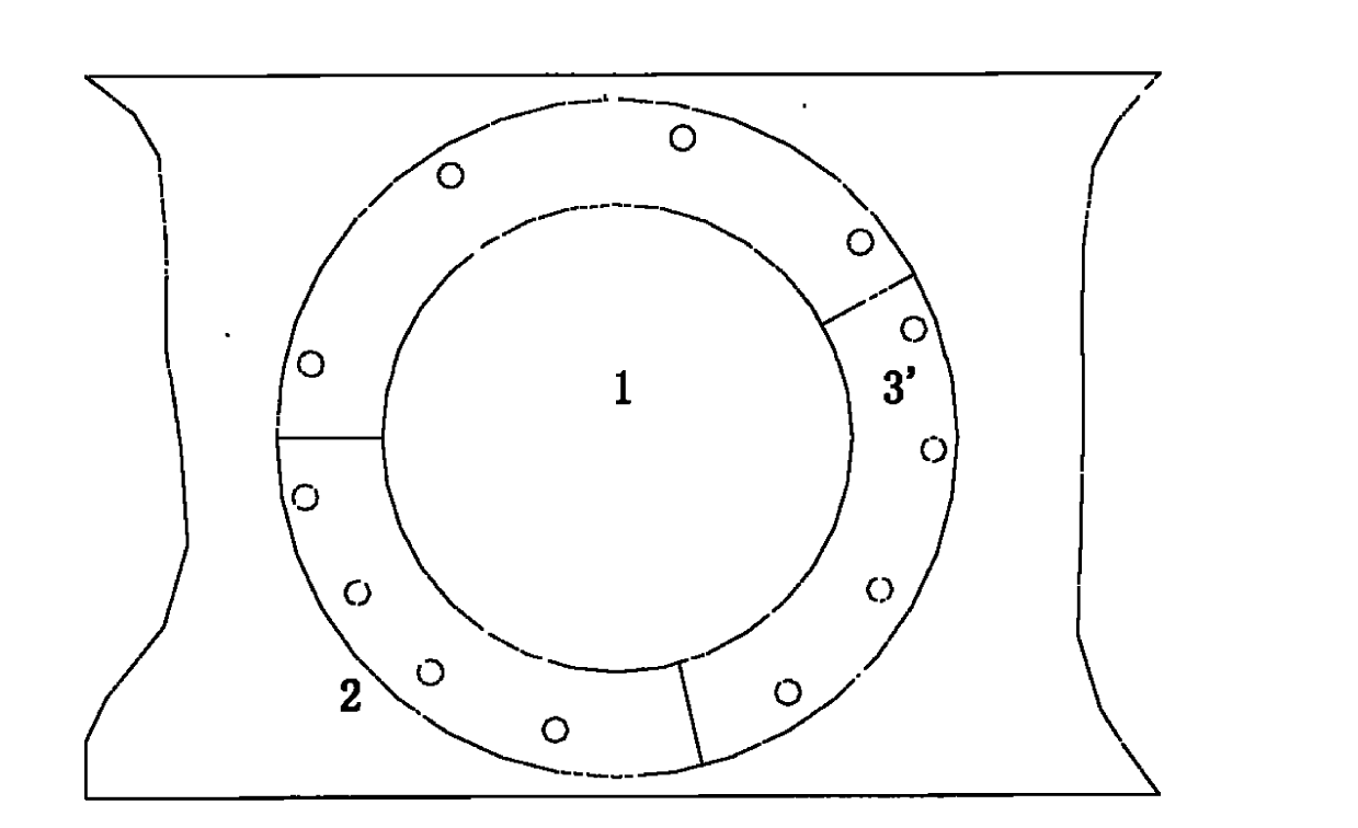
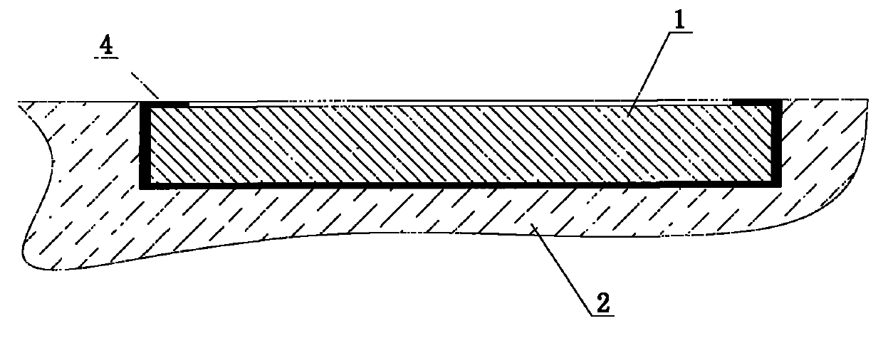
[0038] Embodiment 1 In the preparation method of the LED epitaxial wafer, a sapphire substrate 1 with a thickness of about 100 μm is placed in a holding tank on a graphite disk 2 for heating, and a plurality of pressing sheets are distributed in a ring around the holding tank, so One end of the pressing sheet is fixed on the graphite disc, and the other end is pressed on the ring-shaped area of ​​the upper end surface of the sapphire substrate except for the epitaxial wafer growth area, and the sapphire substrate is locally applied and causes the substrate to be locally warped. The pressure in the opposite direction of the force keeps the substrate flat.

[0039] The aforementioned pressed sheet is made of a material capable of maintaining the original shape at the aforementioned heating temperature, such as boron nitride.

[0040] refer to Figure 2-3 , the pressing sheet can be a plurality of strip pressing sheets 3, one end of each pressing sheet is fixed on the graphite d...

Embodiment 2

[0042] Example 2 In the preparation method of the LED epitaxial wafer, a 2-inch sapphire substrate with a thickness of about 100 μm is placed in a holding tank on a graphite disk for heating, and a set of The upper end surface of the sleeve is provided with an annular opening, and the annular surface is pressed on the upper end surface of the sapphire substrate along the circumferential direction, and the local pressure on the sapphire substrate is opposite to the direction of the force that causes the local warping of the substrate. , the area on the sapphire substrate corresponding to the opening of the casing is the area reserved for epitaxial wafer growth.

[0043] The aforementioned casing includes at least two parts that can be detached along the horizontal direction.

[0044]The aforementioned casing is made of materials capable of maintaining the original shape at the aforementioned heating temperature, such as graphite, tungsten alloy, boron nitride, and the like.

...


PUM


Abstract

The invention relates to a preparation method and device of an LED epitaxial wafer. The method comprises the following step of applying a pressure which is opposite to the direction of a force capable of resulting in partial warping of a substrate to partial substrate during the process for heating the substrate to grow a single crystal film so as to control the substrate at a flat state. The method is carried out by means of fixed mechanism. The preparation method and device of an LED epitaxial wafer provided by the invention have the advantages that the warping phenomenon of sapphire wafers and the like substrates can be effectively removed at a high temperature, the substrate with a relatively small thickness can be directly applied to epitaxial growth, the substrate material is saved, the normal reduction and the like operations are prevented, the manufacture cost of LED epitaxial wafers is reduced greatly, and the production efficiency and the production yield of LED epitaxial wafer are effectively improved.

Description

technical field [0001] The invention relates to a method and a device for preparing an LED chip in the field of optoelectronic technology, in particular to a method and a device for preparing an LED epitaxial wafer. Background technique [0002] The third-generation semiconductor material GaN has the characteristics of wide bandgap, etc., and blue light and ultraviolet light with shorter wavelengths can be obtained through doping, thus creating a great opportunity for white LEDs to replace current traditional lamps such as incandescent lamps and spotlights and full-color large screens. condition. [0003] In the manufacturing process of GaN-based LEDs and other optoelectronic devices, GaN materials are generally produced by epitaxial growth on substrates such as sapphire wafers under high temperature conditions using MOCVD and other processes. However, common substrate materials, especially sapphire materials, have poor thermal conductivity. After heating, they will warp du...

Claims


Application Information

Patent Timeline
Patent Type & Authority Applications(China)
IPC IPC(8): H01L33/00
Inventor 梁秉文
Owner SUZHOU INST OF NANO TECH & NANO BIONICS CHINESE ACEDEMY OF SCI
Why Eureka
Try Eureka