Wafer warping elimination method and composite substrate

A composite substrate and wafer technology, applied in the direction of electrical components, semiconductor/solid-state device manufacturing, circuits, etc., can solve the problems of increasing device cost, high cost, increasing device process difficulty, etc., to reduce the probability of fragmentation or fragmentation, Easy to identify and locate, and the effect of eliminating warpage

Inactive Publication Date: 2018-06-19
BEIJING PINJIE ELECTRONICS TECH CO LTD
View PDF5 Cites 8 Cited by
  • Summary
  • Abstract
  • Description
  • Claims
  • Application Information

AI Technical Summary

Problems solved by technology

[0006] First, the warpage prevents smooth focused exposure of the entire wafer during the lithography process
[0007] Second, warpage makes it difficult for a large number of semiconductor equipment including exposure machines to automatically handle wafers
[0010] One is to increase the cost of devices based on silicon carbide materials. The greater the thickness of the silicon carbide substrate, the more materials consumed by a single wafer,

Method used


Image

  • Wafer warping elimination method and composite substrate
  • Wafer warping elimination method and composite substrate
  • Wafer warping elimination method and composite substrate

Examples


Example Embodiment

[0041] Example 1

[0042] This implementation provides a method for eliminating wafer warpage, which includes the following steps:

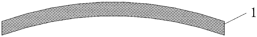
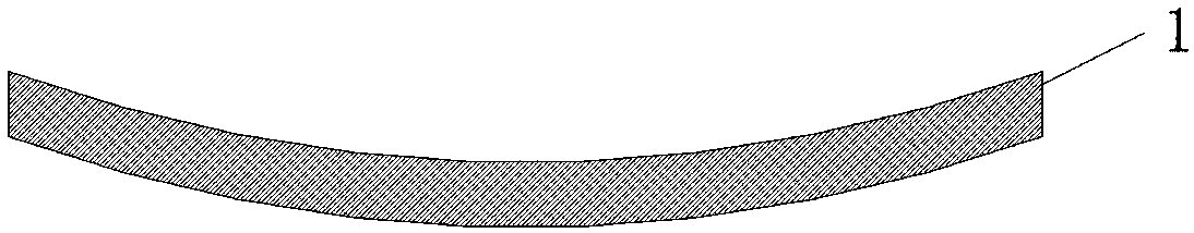
[0043] S1: Select a warped wafer 1;
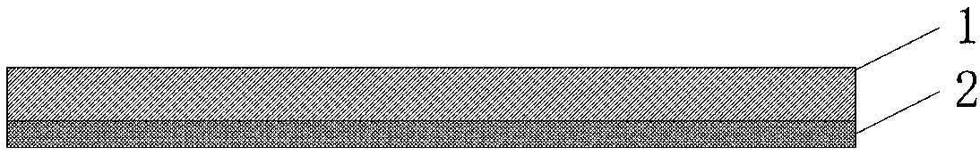
[0044] S2: Depositing a layer of stress compensation film 2 with internal stress on the back surface of the aforementioned wafer 1, so that the internal stress of the stress compensation film 2 and the internal stress of the wafer 1 cancel each other out to obtain a flat composite substrate.

[0045] The aforementioned wafer 1 is a silicon carbide-based silicon carbide wafer or a silicon-based gallium nitride wafer.

[0046] The material of the stress compensation film 2 is preferably silicon oxide, silicon nitride or metal.

[0047] The internal stress of the stress compensation film 2 is compressive stress, non-stress or tensile stress. Those skilled in the art can adjust the type of internal stress (compressive stress, no stress or tensile stress) of the deposited stress compensation film 2 by adjusting the process ...

Example Embodiment

[0050] Example 2

[0051] This implementation provides a method for eliminating wafer warpage, which includes the following steps:

[0052] S1: Select a warped wafer 1;

[0053] S2: Depositing a layer of stress compensation film 2 with internal stress on the back surface of the above-mentioned wafer 1, so that the internal stress of the stress compensation film 2 and the internal stress of the wafer 1 cancel each other out to obtain a flat composite substrate.

[0054] The aforementioned wafer 1 is a silicon carbide-based silicon carbide wafer or a silicon-based gallium nitride wafer.

[0055] The material of the stress compensation film 2 is preferably silicon oxide, silicon nitride or metal.

[0056] The internal stress of the stress compensation film 2 is compressive stress, non-stress or tensile stress. Those skilled in the art can adjust the type of internal stress (compressive stress, tensile stress or no stress) of the deposited stress compensation film 2 by adjusting the process...

Example Embodiment

[0059] Example 3

[0060] This implementation provides a method for eliminating wafer warpage, which includes the following steps:

[0061] S1: Select a warped wafer 1;

[0062] S2: Deposit a layer of stress compensation film 2 with internal stress on the back surface of the above-mentioned wafer 1, so that the internal stress of the stress compensation film 2 and the internal stress of the wafer 1 cancel each other out to obtain a flat composite substrate;

[0063] S3: Deposit a layer of auxiliary film 3 without internal stress on the back surface of the stress compensation film 2.

[0064] The aforementioned wafer 1 is a silicon carbide-based silicon carbide wafer.

[0065] The material of the stress compensation film 2 is preferably silicon oxide, silicon nitride or metal.

[0066] The internal stress of the stress compensation film 2 is compressive stress, non-stress or tensile stress. Those skilled in the art can adjust the type of internal stress (compressive stress, zero stress, o...


PUM


Abstract

The invention discloses a wafer warping elimination method and a composite substrate. The method comprises steps that S1, a warped wafer (1) is selected; S2, a stress compensation film (2) internallyhaving the stress is deposited at a back surface of the wafer (1), and the internal stress of the stress compensation film (2) is made to offset the internal stress of the wafer (1) to acquire a flatcomposite substrate; and the wafer (1) is a silicon carbide based silicon carbide wafer or a silicon-based gallium nitride wafer; the composite substrate comprises the wafer (1) and the stress compensation film (2), wherein the stress compensation film (2) covers the back surface of the wafer (1), the internal stress of the stress compensation film (2) is made to offset the internal stress of thewafer (1), and the wafer (1) is the silicon carbide based silicon carbide wafer or the silicon-based gallium nitride wafer. The wafer warping elimination method is advantaged in that the stress compensation film internally having the stress is deposited at the back surface of the warped wafer, the internal stress of the stress compensation film (2) is made to offset the internal stress of the wafer (1), and the warping phenomenon is eliminated.

Description

technical field [0001] The invention belongs to the technical field of semiconductor micro-nano processing, and in particular relates to a method for eliminating wafer warpage and a composite substrate prepared by the method. Background technique [0002] Silicon carbide (SiC) and gallium nitride (GaN) are two wide bandgap semiconductor materials. They have the advantages of high critical breakdown electric field strength, high saturation electron mobility, high thermal conductivity, etc., and are especially suitable for applications in microwave and high-power In the field of power transmission and energy conversion, microwave devices and power electronic devices prepared with it can carry high voltage and high current, and can work stably in harsh application environments such as high radiation and high temperature. [0003] When the ingot of the silicon carbide substrate grows, the internal stress formed by the silicon carbide crystal is relatively large. When the silico...

Claims


Application Information

Patent Timeline
IPC IPC(8): H01L21/02H01L29/16
CPCH01L21/02016H01L29/1608
Inventor 何钧
Owner BEIJING PINJIE ELECTRONICS TECH CO LTD
Why Eureka
Try Eureka