Restoration device and restoration method for storage chip

A memory chip and storage module technology, applied in static memory, instruments, etc., can solve problems such as memory chip repair failure, violation of parallel testing, and memory chip repair speed reduction, achieving the goal of reducing test time, increasing speed, and increasing success rate Effect

Active Publication Date: 2012-07-18
GIGADEVICE SEMICON (BEIJING) INC
View PDF5 Cites 25 Cited by
  • Summary
  • Abstract
  • Description
  • Claims
  • Application Information

AI Technical Summary

Problems solved by technology

[0005] It can be seen that in order to record the error addresses of different memory chips, the existing memory chip repair method needs to read each memory chip serially; The serial repair of each memory chip is performed at the wrong address, which violates the original intention of parallel testing, resulting in a reduction in the repair speed of memory chips
[0006] In addition, due to the hardw

Method used


Image

  • Restoration device and restoration method for storage chip
  • Restoration device and restoration method for storage chip
  • Restoration device and restoration method for storage chip

Examples


Embodiment 2

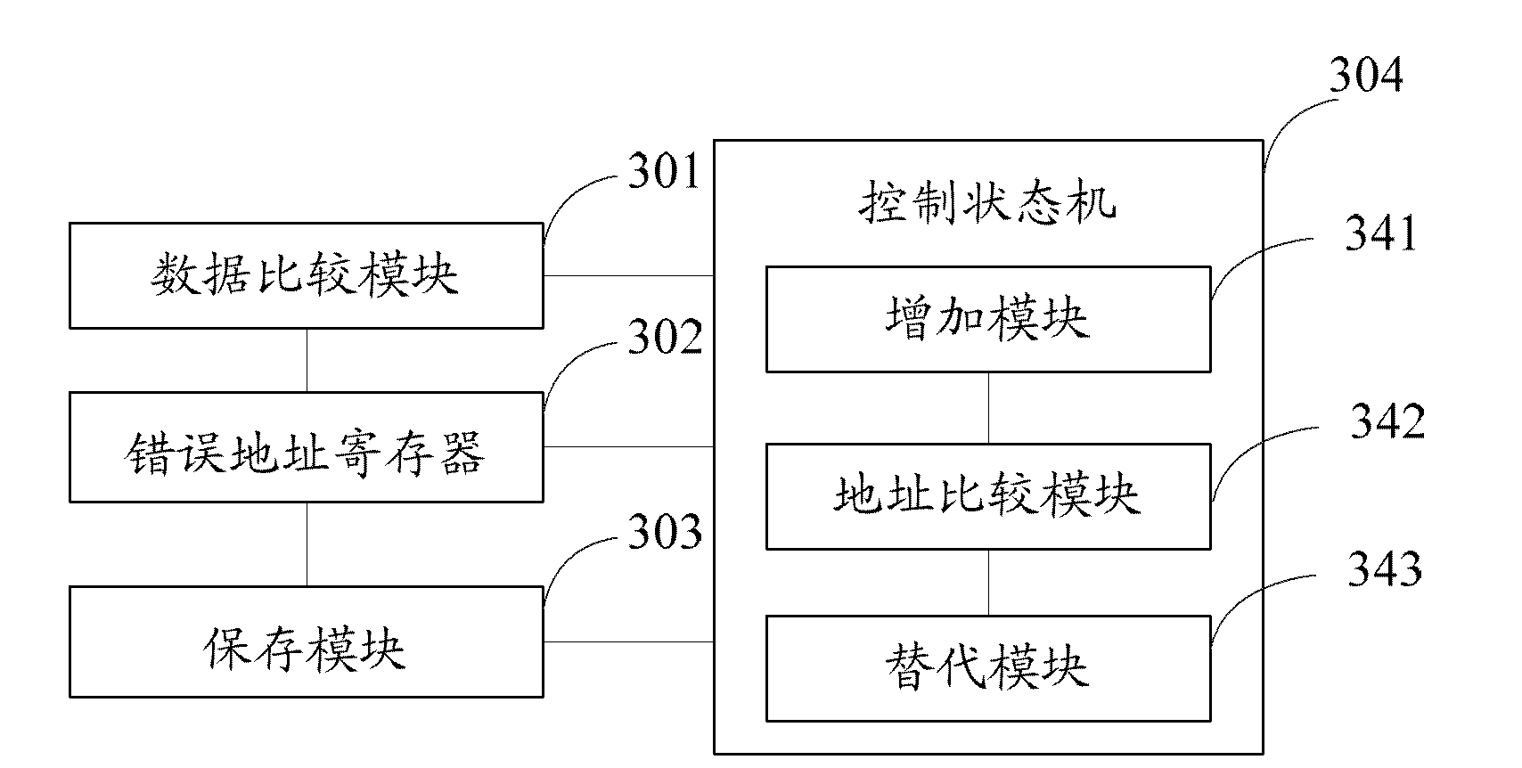
[0092] Compared with Embodiment 2, the control state machine 304 of this embodiment can not only automatically record and store the error address of each memory chip when the ATE reads the memory chips in parallel, but also realize the repair of the memory chips.

[0093] Assuming that the number of existing normal memory cell arrays in the memory chip is 1024, then the adding module 341 can increase some extra address space by adding a certain number (for example, the number is 16) of backup cells, namely redundancy (redundancy) space.

[0094] Because the saving module 303 can permanently save the wrong address checked out in the repair process, then, in the process of using the memory chip by the user, the wrong address saved in the saving module can be compared with the address input by the user, and the wrong The space corresponding to the address is turned off and replaced with redundant space.

[0095] In the existing method of background technology, the memory chip is...


PUM


Abstract

The invention provides a restoration device and a restoration method for a storage chip. The restoration device is positioned inside the storage chip, and comprises a data comparison module, a misaddress register and a saving module, wherein the data comparison module is used for comparing data in a current address of the storage chip with preset target data when the storage chip is read in parallel by using automatic testing equipment; the misaddress register is used for recording the current address as a misaddress when data in the current address is different from the preset target data; and the saving module is used for saving the misaddress in the misaddress register after the storage chip is read. According to the device and the method, parallel restoration of the storage chip can be realized, and the restoration speed and success rate of the storage chip can be increased.

Description

technical field [0001] The invention relates to the technical field of semiconductor chips, in particular to a repairing device and method for a memory chip. Background technique [0002] With the rapid development of microelectronics technology, parallel chip testing has been introduced into integrated circuit fields such as printed circuit boards, communication products and system-on-chips, and has been widely used. Parallel chip testing refers to completing multiple test tasks at the same time, including completing the testing of multiple chips under test at the same time, or running multiple test tasks asynchronously or synchronously on a single chip under test, and completing the test tasks at the same time Measurement of multiple parameters of the chip. [0003] The basic storage unit of a memory chip is a memory cell. In order to ensure the safety and reliability of the data in the memory chip, it usually does not allow a memory cell to be damaged. Therefore, in the ...

Claims


Application Information

Patent Timeline
IPC IPC(8): G11C29/44
Inventor 苏志强舒清明
Owner GIGADEVICE SEMICON (BEIJING) INC
Why Eureka
Try Eureka