

Method for measuring junction temperature and thermal resistance of metal-oxide semiconductor tube
A semiconductor tube and measurement method technology, applied in the direction of single semiconductor device testing, material thermal development, etc., can solve problems such as multi-time, high cost, and complicated operation methods, and achieve the effect of simple operation, low cost, and wide application range
- Summary
- Abstract
- Description
- Claims
- Application Information
AI Technical Summary
Problems solved by technology
Method used
Image

Examples
Embodiment Construction
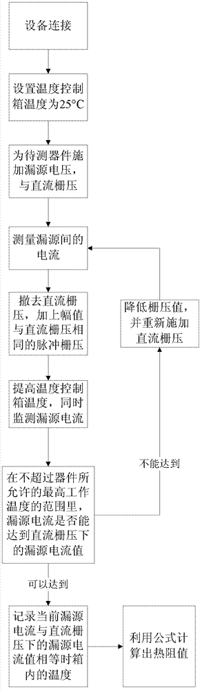
[0032] A method for measuring the junction temperature and thermal resistance of metal oxide semiconductor tubes,
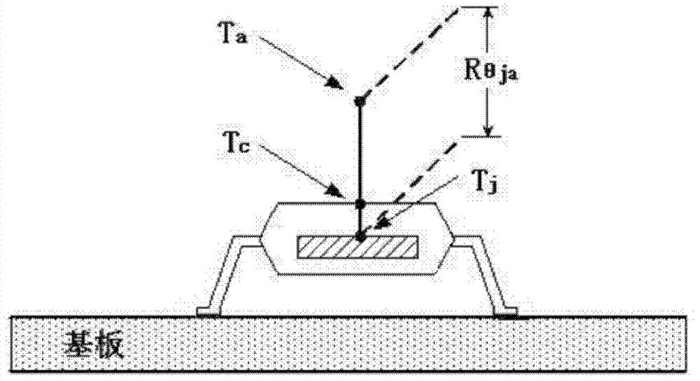
[0033] Step 1 Place the insulating substrate with the device under test in the temperature control box, and adjust the temperature control box to 25°C. According to the range of the safe working area of the device under test, and ensure that the device under test can work normally, give A DC voltage is applied across the drain-source of the device under test,
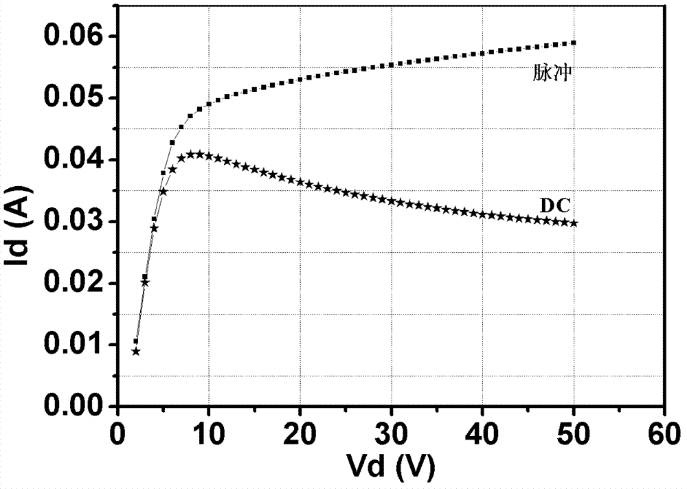
[0034] Step 2: Apply a grid DC operating voltage on the grid, and measure the current at both ends of the drain and source of the device under test when the voltage on the grid is a DC operating voltage,
[0035] Step 3 remove the DC operating voltage on the grid, and then apply a square wave pulse voltage on the grid, the amplitude of the square wave pulse voltage is equal to the DC operating voltage described in step 2, the duty cycle is less than 1% and the period is not Greater than 1 millisecond, i...
PUM
| Property | Measurement | Unit |
|---|---|---|
| current | aaaaa | aaaaa |
Abstract
Description
Claims
Application Information