Display panel and manufacturing method thereof

一种显示面板、制作方法的技术,应用在半导体/固态器件制造、半导体器件、电气元件等方向

Inactive Publication Date: 2012-08-01
AU OPTRONICS CORP
View PDF4 Cites 32 Cited by
  • Summary
  • Abstract
  • Description
  • Claims
  • Application Information

AI Technical Summary

Problems solved by technology

However, when it is applied to a larger-sized display panel, the area of ​​the upper electrode formed by a thin metal layer or a transparent conductive layer needs to be enlarged accordingly, so internal resistance is likely to occur in the far-distance areas on the display panel. The phenomenon of IR drop causes problems in the uniformity of luminous brightness between regions on the display panel, and thus limits the application of organic light-emitting diode displays in large-size display devices.

Method used


Image

  • Display panel and manufacturing method thereof
  • Display panel and manufacturing method thereof
  • Display panel and manufacturing method thereof

Examples


Embodiment Construction

[0029] In order to enable those who are familiar with the technical field of the present invention to further understand the present invention, the preferred embodiments of the present invention are listed below, together with the accompanying drawings, to describe in detail the composition of the present invention and the desired effects .

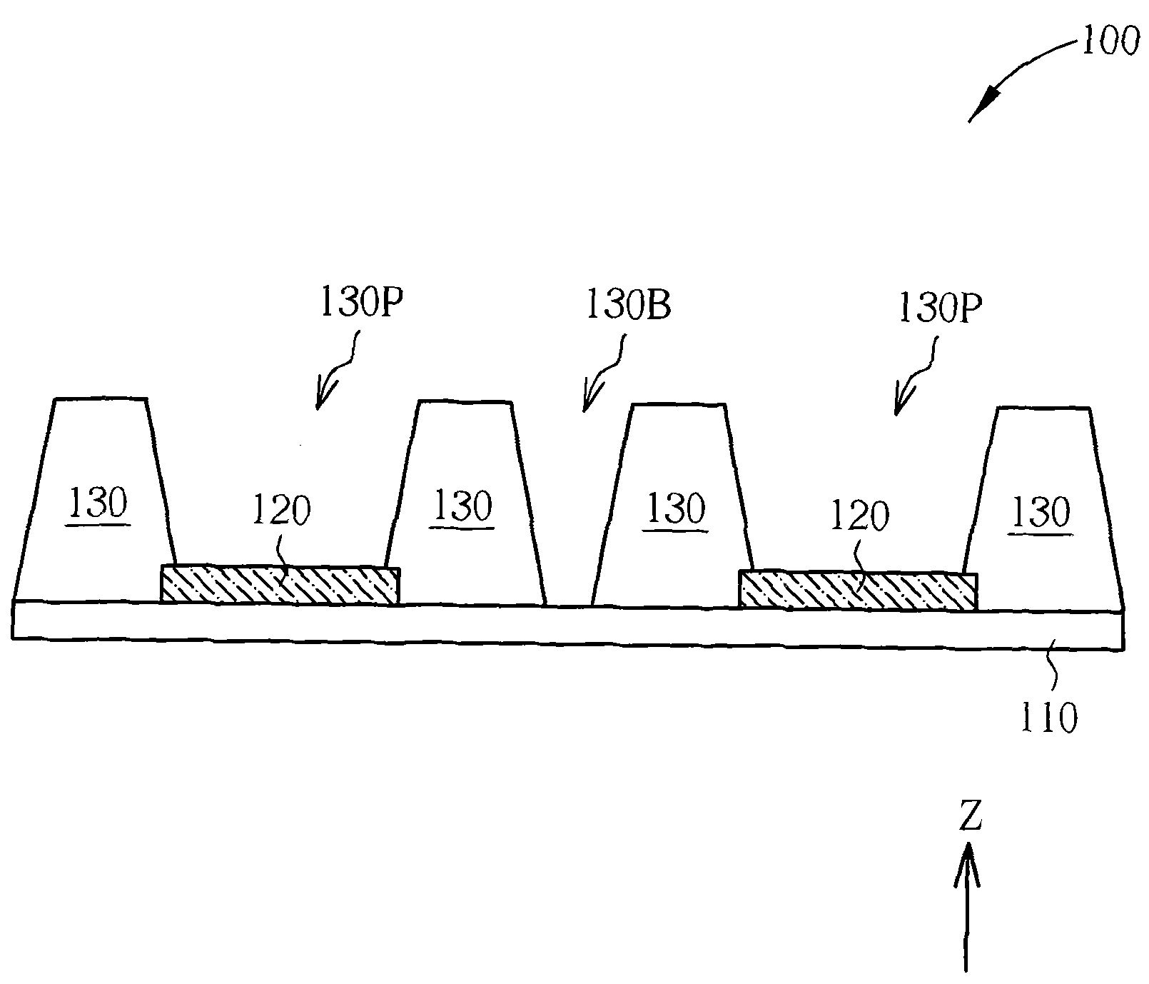
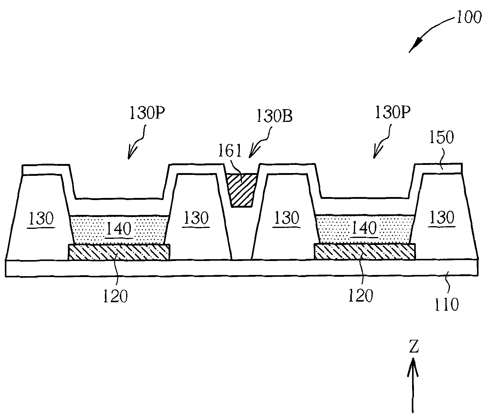
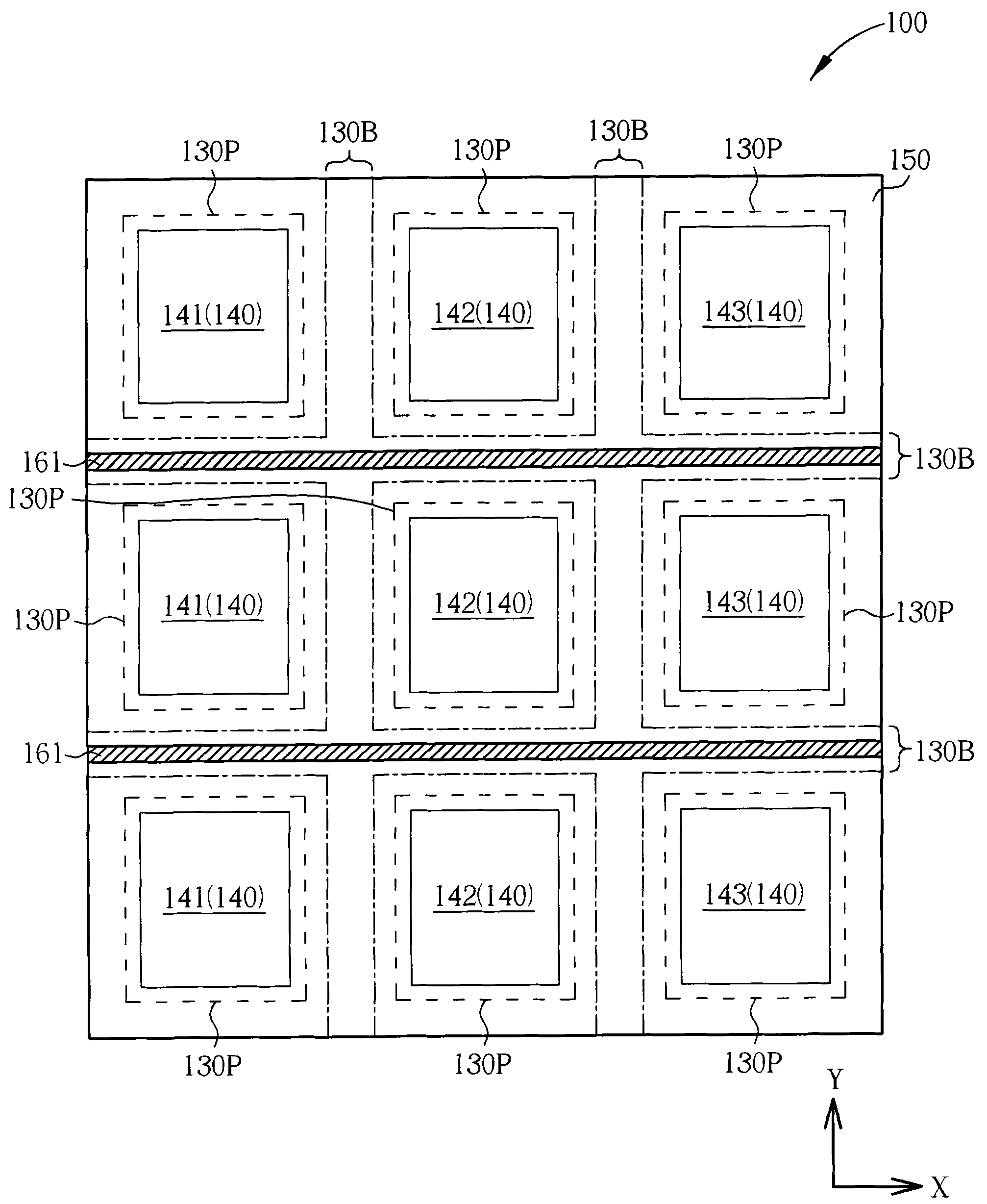
[0030] Please refer to Figure 1A , Figure 1B , Figure 2A , Figure 2B and Figure 2C . Figure 1A , Figure 1B as well as Figure 2A A schematic diagram of a manufacturing method of a first preferred embodiment of the display panel of the present invention is shown. in Figure 1A and Figure 1B is a side view, and Figure 2A for the top view. Figure 2B A schematic top view showing another preferred implementation of the auxiliary electrode of the display panel of the present invention, Figure 2C A schematic top view of another preferred implementation of the auxiliary electrode of the display panel of the present invention i...


PUM


Abstract

The invention discloses a display panel and a manufacturing method thereof. The display panel comprises a substrate, multiple lower electrodes, a separating layer, multiple light-emitting layers, an upper electrode and at least a first auxiliary electrode. The lower electrodes and the separating layer are arranged on the substrate. The separating layer has multiple pixel region openings and at least one buffer region. The pixel region openings expose the corresponding lower electrodes, respectively. The buffer region is disposed between two adjacent pixel region openings. The light-emitting layers are arranged on the corresponding lower electrodes, respectively. The upper electrode covers the light-emitting layers, the separating layer and the buffer layer. The first auxiliary electrode is provided in the buffer layer.

Description

technical field [0001] The invention relates to a display panel and a manufacturing method thereof, in particular to a display panel with auxiliary electrodes and a manufacturing method thereof. Background technique [0002] Electroluminescent display device (electroluminescent display device) has been expected to replace liquid crystal display and become the next generation due to its characteristics such as no need for color filter, self-illumination (no backlight module required) and low power consumption. Generations of mainstream display technology. Among various electroluminescence displays, an organic light emitting diode display is one of relatively mature technologies at present. [0003] Generally, OLED displays can be classified into top emission OLED displays and bottom emission OLED displays according to their structural design and light emission direction. In the structure of the top-emission organic light-emitting diode display, in order to increase the tran...

Claims


Application Information

Patent Timeline
Patent Type & Authority Applications(China)
IPC IPC(8): H01L51/52H01L27/32H01L51/56
CPCH01L27/3283H01L27/3246H01L51/52H01L27/329H01L27/3279H01L51/56H01L27/32H10K59/173H10K59/1795H10K59/1315H10K59/122H10K50/80H10K59/00H10K71/00
Inventor 陈鹏聿蔡纶陈之磊周书伃
Owner AU OPTRONICS CORP
Why Eureka
Try Eureka