

Automatic aperture control device and automatic aperture control method of full HD (High-Definition) camera
A high-definition camera and automatic aperture technology, which is applied to control exposure, optics, cameras, etc., can solve problems such as inaccurate aperture positions, and achieve the effects of simple circuit implementation, accurate aperture control, and cost reduction
- Summary
- Abstract
- Description
- Claims
- Application Information
AI Technical Summary
Problems solved by technology
Method used
Image

Examples
Embodiment 1
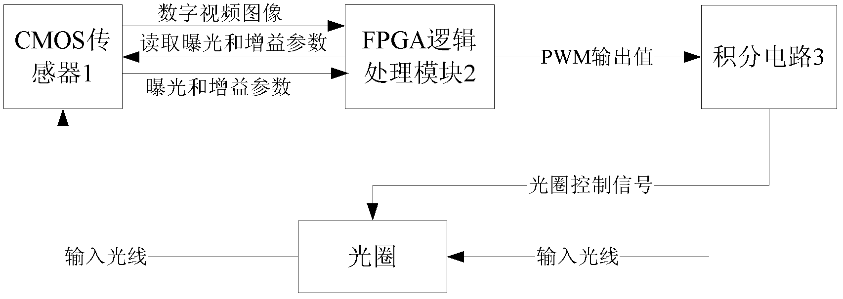
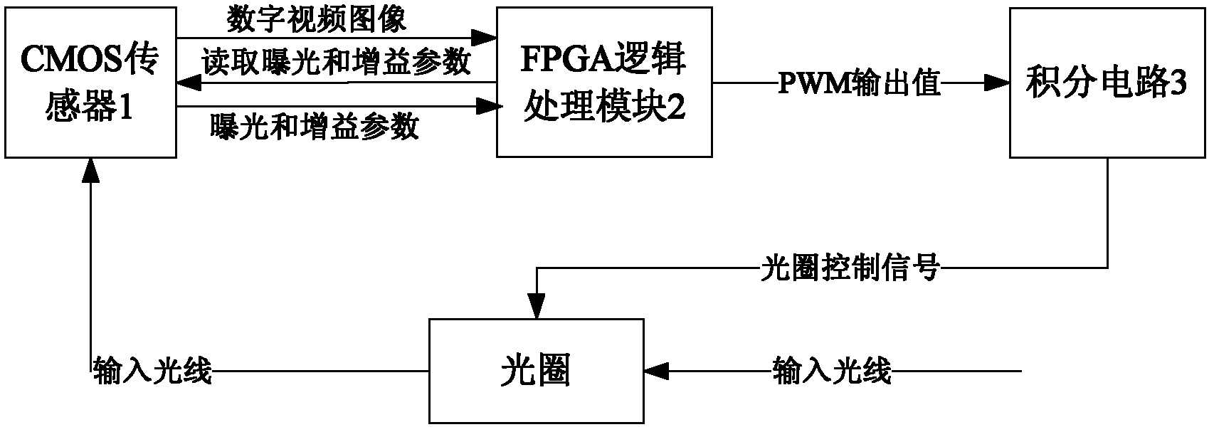
[0044] An automatic aperture control device for a full high-definition camera, including sequentially connected CMOS sensors (such as HD CMOS sensors) 1, a computing module, and an auxiliary device that assists the computing module to control the aperture. For example, if the computing module includes digitally controlled The analog circuit is a PWM (pulse width modulation) output value calculation module for controlling the aperture, then the auxiliary equipment that needs to be connected to the operation module is an integral circuit that converts the PWM output value to an analog voltage value, and the analog voltage value can control the opening of the aperture to the proper location. In this way, compared with the automatic aperture control device which uses the D / A conversion chip and its driving circuit as auxiliary equipment and does not have a PWM output value calculation module in the calculation module, the cost and power consumption of the system can be greatly redu...
Embodiment 2
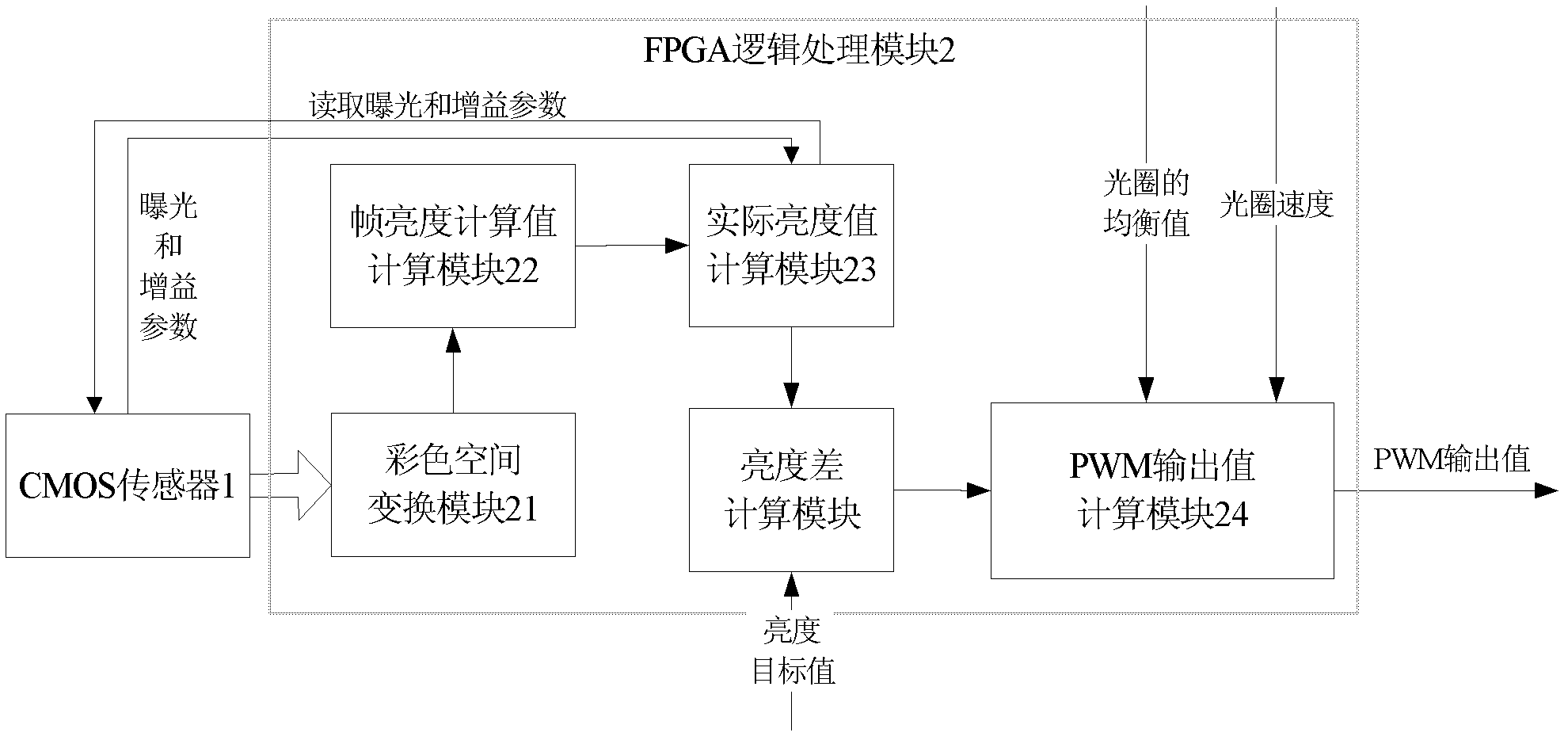
[0051] A kind of automatic aperture control device of full high-definition video camera, comprises CMOS sensor 1 and operation module (similar to embodiment 1, can be FPGA logic processing module 2, CPLD logic gate or other ASIC device equally); The setting of described CMOS sensor 1 And function is the same as embodiment 1, also is arranged on lens rear, receives the input light that enters by the aperture of lens to make it form digital video image; CMOS sensor is connected with operation module, and the frame of CMOS sensor output digital video image is to operation module , the CMOS sensor has an exposure setting, and an exposure parameter and a gain parameter of a frame are calculated through the exposure setting. In this embodiment, the auxiliary equipment is a D / A conversion chip and its driving circuit; the CMOS sensor is sequentially connected with the operation module, the D / A conversion chip and its driving circuit. In this embodiment, the calculation module include...
Embodiment 3
[0055] On the basis of the structure of the above-mentioned embodiment 1 and embodiment 2, this embodiment proposes a preferred specific implementation method for accurately calculating the brightness gain: the exposure parameter includes the number of exposure lines exp_line, and the gain parameter includes the analog gain analog_gain and Digital gain digital_gain, the luminance gain, that is, the exposure and gain compensation value exposure is obtained by the formula exposure=exp_line×analog_gain×digital_gain (can be performed in the FPGA logic processing module 2).
[0056]If the unit conversion in practice is taken into account, that is, the gain (in dB) is converted into a multiple, then the brightness gain, that is, the exposure and gain compensation value exposure can be obtained by the formula exposure=exp_line×(analog_gain×Na)×(digital_gain×Nd ), where Na is the proportional coefficient of the analog gain, and Nd is the proportional coefficient of the digital gain. F...
PUM
 Abstract
Description
Claims
Application Information