Array substrate, manufacturing method of array substrate, liquid crystal panel and liquid crystal display

A technology of array substrate and base substrate, which is applied in the field of array substrate and manufacturing method, liquid crystal panel and liquid crystal display, can solve the problems of increasing data line driving power consumption, restricting the development and application of large-size liquid crystal display panel, etc. The effect of power consumption

Active Publication Date: 2012-08-08
BOE TECH GRP CO LTD +1
View PDF4 Cites 22 Cited by
  • Summary
  • Abstract
  • Description
  • Claims
  • Application Information

AI Technical Summary

Problems solved by technology

In the existing technology, in order to realize dot inversion, it is necessary to continuously invert the working voltage of each pixel unit driven by the data line within the same frame time, and the frequent alternating changes of the working voltage between high and low voltages lead to an increase in the power consumption of the data line drive, which limits Development and application of large-size liquid crystal display panels

Method used


Image

  • Array substrate, manufacturing method of array substrate, liquid crystal panel and liquid crystal display
  • Array substrate, manufacturing method of array substrate, liquid crystal panel and liquid crystal display
  • Array substrate, manufacturing method of array substrate, liquid crystal panel and liquid crystal display

Examples


Embodiment Construction

[0039] The following will clearly and completely describe the technical solutions in the embodiments of the present invention with reference to the accompanying drawings in the embodiments of the present invention. Obviously, the described embodiments are only some, not all, embodiments of the present invention. Based on the embodiments of the present invention, all other embodiments obtained by persons of ordinary skill in the art without making creative efforts belong to the protection scope of the present invention.

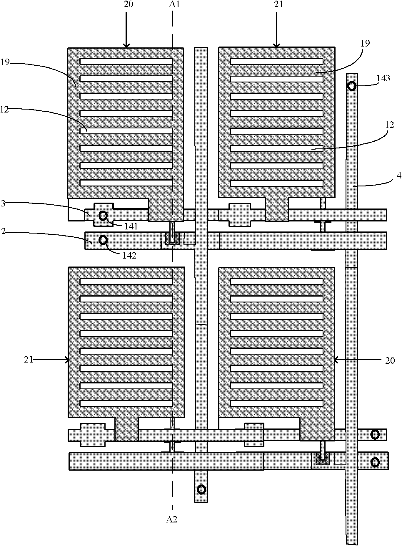
[0040]In all the embodiments of the present invention, the arrangement on the same layer refers to at least two patterns, and refers to a structure in which at least two patterns are arranged on the same layer of film. Specifically, the at least two patterns are formed on a film made of the same material through a patterning process. For example, the manufacturing process of setting the grid line and the gate line in the same layer may be: using molybdenum, co...


PUM


Abstract

The invention discloses an array substrate, a manufacturing method of the array substrate, a liquid crystal panel and a liquid crystal display, relates to the technical field of liquid crystal display, and aims to reduce the driving power consumption required by reverse driving. The array substrate comprises a substrate base plate, grid lines, data lines and pixel units; each pixel unit comprises two layers of transparent conducting films and a thin film transistor; the pixel units are divided into first pixel units and second pixel units; the first pixel units and the second pixel units are arranged at intervals in the directions of the data lines; in each first pixel unit, the first layer of transparent conducting film is electrically connected with a corresponding common electrode wire, and the second layer of transparent conducting film is electrically connected with a drain electrode of the corresponding thin film transistor; in each second pixel unit, the first layer of transparent conducting film is electrically connected with the drain electrode of the corresponding thin film transistor, and the second layer of transparent conducting film is electrically connected with the corresponding common electrode wire; and the common electrode wires in all the pixel units are electrically connected. The array substrate, the manufacturing method of the array substrate, the liquid crystal panel and the liquid crystal display are applied to the technical field of the liquid crystal display.

Description

technical field [0001] The invention relates to liquid crystal display technology, in particular to an array substrate and a manufacturing method, a liquid crystal panel and a liquid crystal display. Background technique [0002] A liquid crystal display is a commonly used flat panel display at present, and a Thin Film Transistor Liquid Crystal Display (TFT-LCD for short) is a mainstream product in the liquid crystal display. TFT-LCD is generally made by combining the array substrate and the color filter substrate and filling the liquid crystal layer between them. The twist of the liquid crystal molecules is driven by an electric field, so that light selectively passes through to present images of different gray scales. An electric field driving liquid crystal molecules to twist is formed between the pixel electrode and the common electrode. The common electrode is connected with the common electrode line, and the common voltage is input through the common electrode line; ...

Claims


Application Information

Patent Timeline
Patent Type & Authority Applications(China)
IPC IPC(8): G02F1/1362G02F1/1368G02F1/133H01L21/77H01L27/12
CPCH01L27/1214G02F1/136286G09G3/36G09G3/3614G09G3/3648G09G2300/0426G09G2320/0252G02F1/134372H01L27/124G02F1/1368G02F1/13685H01L27/1251H01L27/1262
Inventor 刘莎王宝强
Owner BOE TECH GRP CO LTD
Why Eureka
Try Eureka