Low-grid charge power device and manufacturing method thereof

A power device and charge technology, applied in the fields of semiconductor/solid-state device manufacturing, electrical components, semiconductor devices, etc., can solve the problems of increasing the driving power consumption of switching devices, reducing gate charge, gate charge, etc., so as to reduce the driving power. consumption, gate charge reduction, and simple process steps

Inactive Publication Date: 2014-04-16
HANGZHOU LION MICROELECTRONICS CO LTD
View PDF2 Cites 5 Cited by
  • Summary
  • Abstract
  • Description
  • Claims
  • Application Information

AI Technical Summary

Problems solved by technology

[0007] The purpose of the present invention is to solve the problem that the gate charge (Qg) of the power device in the prior art is relatively high, and the capacitance between the gate region and the drain is large, which will significantly increase the driving power consumption of the switching device, and provides a low gate In the charge power device, the gate oxide layer in the device of the present invention includes a main gate oxide layer and a sub-gate oxide layer, and a stepped structure is formed between the sub-gate oxide layer and the main gate oxide layer. By increasing the thickness of the main gate oxide layer, the In the case of affecting the switching speed of the device, the capacitance between the gate region and the drain is reduced to reduce the gate charge

Method used


Image

  • Low-grid charge power device and manufacturing method thereof
  • Low-grid charge power device and manufacturing method thereof
  • Low-grid charge power device and manufacturing method thereof

Examples


Embodiment 1

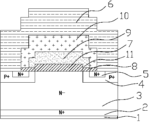
[0040] Such as figure 1 As shown, a low gate charge power device includes a drain 1 with a thickness of 5000 angstroms, an N+ type substrate 2 on the drain 1 and an N-type drift region 3 on the N+ type substrate 2, The shoulders on both sides of the N-type drift region 3 are provided with a P+ type channel region 4, the top surface of the P+ type channel region 4 is provided with an N+ type source region 5, and the N-type drift region 3 is provided with a gate region, A source 6 is provided on the gate region, and the gate region includes a gate oxide layer located on the N-type drift region 3. A polysilicon gate 9 is provided on the gate oxide layer. An ILD insulating layer 10 is provided on the polysilicon gate 9. The gate oxide layer includes The main gate oxide layer 7 with a thickness of 3000 angstroms and the sub-gate oxide layer 8 with a thickness of 800 angstroms located on both sides of the main gate oxide layer 7, the main gate oxide layer 7 is located above the N-ty...

Embodiment 2

[0052] The structure of the low gate charge power device of this embodiment is exactly the same as that of Embodiment 1, except that the drain 1 has a thickness of 12000 angstroms, the main gate oxide layer 7 has a thickness of 4000 angstroms, and the sub-gate oxide layer 8 The thickness of the gate oxide layer 7 is 900 angstroms, and the width of the main gate oxide layer 7 is smaller than the width of the top surface of the N-type drift region 3 .

[0053] The preparation method of the low gate charge power device of this embodiment is exactly the same as that of Embodiment 1, except that: an N-type epitaxial layer with a thickness of 20 μm and a resistivity of 30 Ω / □ is formed on the N+ type substrate 2, and boron The ion source of ion implantation is 11B+, the implantation energy is 100KeV, and the implantation dose is 4.0E13 ions / cm 2 , the ion source of phosphorus ion implantation is 31P+, the implantation energy is 130KeV, and the implantation dose is 3.0E15 ions / cm 2 ...

Embodiment 3

[0056] The structure of the low gate charge power device of this embodiment is exactly the same as that of Embodiment 1, except that the thickness of the drain 1 is 15,000 angstroms, the thickness of the main gate oxide layer 7 is 8,000 angstroms, and the thickness of the sub-gate oxide layer 8 The thickness is 1500 angstroms, and the width of the main gate oxide layer 7 is equal to the width of the top surface of the N-type drift region 3 .

[0057] The preparation method of the low gate charge power device of this embodiment is exactly the same as that of Embodiment 1, except that: an N-type epitaxial layer with a thickness of 60 μm and a resistivity of 40 Ω / □ is formed on the N+ type substrate 2, and boron The ion source of ion implantation is 11B+, the implantation energy is 120KeV, and the implantation dose is 6.0E13 ions / cm 2 , the ion source of phosphorus ion implantation is 31P+, the implantation energy is 160KeV, and the implantation dose is 8.0E15 ions / cm 2 .

[00...


PUM


Abstract

The invention discloses a low-grid charge power device. A combined type grid oxidation layer composed of a primary grid oxidation layer and a secondary grid oxidation layer is adopted in a grid oxidation layer of a grid area, a step structure is formed between the secondary grid oxidation layer and the primary grid oxidation layer, the width of the primary grid oxidation layer is smaller than or equal to the width of the top face of an N- type drift area, the thickness of the primary grid oxidation layer can be independently increased so that the overall thickness of the grid oxidation layer can be increased and the vertical thickness of the secondary grid oxidation layer in contact with a channel cannot be influenced, therefore, the capacitance between the grid area and a drain electrode is reduced under the premise of not influencing the turn-on and turn-off speed of the device, the aim of reducing grid charges is achieved, and the drive power consumption of turning on and off the device is lowered. The invention further discloses a manufacturing method of the low-grid charge power device. Under the condition of being compatible with an existing process, the primary grid oxidation layer and the secondary grid oxidation layer are formed successively by two steps to obtain the combined type grid oxidation layer, the process steps are simple, and operability is strong.

Description

technical field [0001] The invention relates to the technical field of semiconductors, in particular to a low gate charge power device and a preparation method thereof. [0002] Background technique [0003] Power Metal-Oxide-Semiconductor Field Effect Transistor (Power MOSFET) structure has a wide range of applications in a very wide range of fields due to its functional specificity. For example, disk drives, automotive electronics, and power devices. Take power devices as an example, such as VDMOS (Vertical double-diffused metal oxide semiconductor, vertical double-diffused MOS). VDMOS is a voltage-controlled device. Under the control of a suitable gate voltage, the surface of the semiconductor is reversed to form a conductive channel. The channel, so the right amount of current flows vertically between the drain and source. [0004] When the traditional VDMOS device is working, the channel is formed on both sides of the gate region. This structure has a large contact p...

Claims


Application Information

Patent Timeline
Patent Type & Authority Applications(China)
IPC IPC(8): H01L29/78H01L29/423H01L21/336H01L21/28
CPCH01L29/7802H01L21/28158H01L29/42364H01L29/66712
Inventor 王海峰张瑞丽石夏雨邱涛陈祖银
Owner HANGZHOU LION MICROELECTRONICS CO LTD
Why Eureka
Try Eureka