Array substrate, liquid crystal display device and repairing method of liquid crystal display device

An array substrate and repair line technology, applied in the field of liquid crystal display, can solve problems such as dust pollution, no signal input of data lines, and process complexity

Active Publication Date: 2012-08-29
BOE TECH GRP CO LTD +1
View PDF5 Cites 21 Cited by
  • Summary
  • Abstract
  • Description
  • Claims
  • Application Information

AI Technical Summary

Problems solved by technology

In the manufacturing process of the above-mentioned array substrate, due to the complexity of the process, instability or dust pollution, etc., the lead wires in the peripheral lead area are often disconnected.
When the display panel is finally formed, these disconnected leads will cause no signal input to the grid lines or data lines connected to the disconnected leads, resulting in poor display of the screen; when the situation is more serious, the entire liquid crystal display panel will be made Scrap treatment, which greatly reduces the product yield and economic benefits

Method used


Image

  • Array substrate, liquid crystal display device and repairing method of liquid crystal display device
  • Array substrate, liquid crystal display device and repairing method of liquid crystal display device
  • Array substrate, liquid crystal display device and repairing method of liquid crystal display device

Examples


Embodiment Construction

[0022] The following will clearly and completely describe the technical solutions in the embodiments of the present invention with reference to the accompanying drawings in the embodiments of the present invention. Obviously, the described embodiments are only some, not all, embodiments of the present invention. Based on the embodiments of the present invention, all other embodiments obtained by persons of ordinary skill in the art without making creative efforts belong to the protection scope of the present invention.

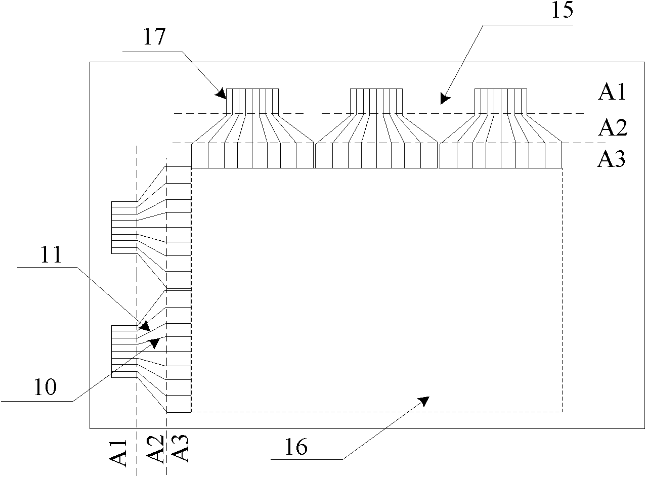
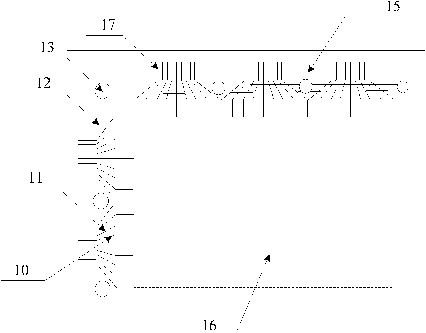
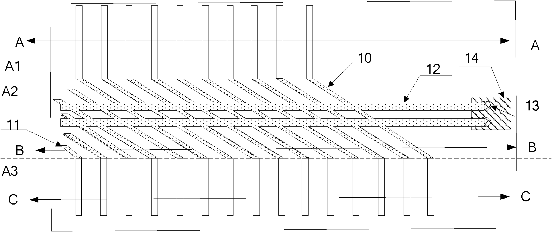
[0023] An embodiment of the present invention provides an array substrate, such as figure 1 As shown, the array substrate includes: an effective display area 16 and a peripheral lead area 15; wherein, leads 11 are formed in the peripheral lead area 15, and a repair line 10 is formed at the corresponding position of each lead 11 in the peripheral lead area 15 , each repair line 10 is electrically connected to the common electrode 14, and an insulating layer is ...


PUM


Abstract

The invention discloses an array substrate, a liquid crystal display device and a repairing method of the liquid crystal display device, relates to the liquid crystal display field and aims at improving the yield of products. The array substrate comprises an active display area and a peripheral lead area. Leads are formed at the peripheral lead area; a repair line is formed at the relevant position of each lead in the peripheral lead area; all the repair lines are electrically connected with a public electrode; and an insulating layer is arranged between the layer on which the leads are located and the layer on which the repair lines are located. The scheme disclosed by the invention is suitable for the production of liquid crystal display panels and liquid crystal display monitors.

Description

technical field [0001] The invention relates to the field of liquid crystal display, in particular to an array substrate, a liquid crystal display device and a repair method thereof. Background technique [0002] Thin Film Transistor-Liquid Crystal Display (TFT-LCD for short) has the advantages of excellent performance, good mass production characteristics, high degree of automation, and low cost of raw materials, and has been widely used in various electronic products. [0003] The liquid crystal display panel includes: a color filter substrate and an array substrate formed in a box; wherein, the effective display area of ​​the array substrate is formed with grid lines and data lines, and a grid line is formed in the peripheral lead area of ​​the array substrate to provide switching scanning signals for the grid lines. wire leads, and data wire leads that provide data scan signals for the data wires. Generally, gate line leads and data line leads can be collectively referr...

Claims


Application Information

Patent Timeline
Patent Type & Authority Applications(China)
IPC IPC(8): G02F1/1362G02F1/13H01L27/02
CPCG02F1/136259G02F1/136263G02F1/136272
Inventor 张洪林王丹邵喜斌
Owner BOE TECH GRP CO LTD
Why Eureka
Try Eureka