Complementary metal oxide semiconductor (CMOS) image sensor and manufacturing method thereof

A technology of an image sensor and a manufacturing method, applied in the semiconductor field, can solve the problems of high power consumption and difficult integration of a CCD image sensor, and achieve the effects of improving image quality and preventing oxidation and enhancing diffusion effect.

Active Publication Date: 2012-08-29
SEMICON MFG INT (SHANGHAI) CORP
View PDF4 Cites 13 Cited by
  • Summary
  • Abstract
  • Description
  • Claims
  • Application Information

AI Technical Summary

Problems solved by technology

The advantage of the CCD image sensor is that it has high image sensitivity and low noise, but it is difficult to integrate the CCD image sensor with other devices, and the power consumption of the CCD image sensor is relatively high.

Method used


Image

  • Complementary metal oxide semiconductor (CMOS) image sensor and manufacturing method thereof
  • Complementary metal oxide semiconductor (CMOS) image sensor and manufacturing method thereof
  • Complementary metal oxide semiconductor (CMOS) image sensor and manufacturing method thereof

Examples


Embodiment Construction

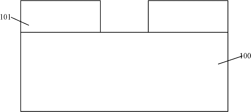
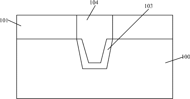
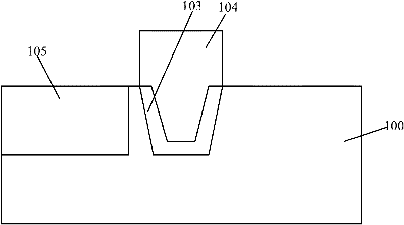
[0034] The imaging quality of existing CMOS image sensors is not high. After research by the inventors, it is found that one of the main reasons for the poor imaging quality of the CMOS image sensor is that the dark current of the CMOS image sensor is relatively large. Specifically, combined with image 3 One of the main causes of dark current is due to the dangling bonds at the interface between the liner layer 103 of the shallow trench isolation structure and the semiconductor substrate 100, and the dangling bonds will be between the liner layer 103 and The interface between the semiconductor substrates 100 forms an interface state defect, so that a large amount of electrons are easily formed on the interface between the pad layer 103 and the semiconductor substrate 100 due to heat generation (the reason for the heat generation is due to the fabrication of semiconductor devices. Various heating processes required in the process, such as oxidation process, annealing process)...


PUM


Abstract

The invention provides an image sensor and a manufacturing method thereof. The manufacturing method comprises the following steps of forming a shallow trench isolation structure in a semiconductor substrate; forming a doping layer surrounding the shadow trench isolation structure in the semiconductor substrate; and forming a photosensitive area of a photoelectric diode at one side of the shadow trench isolation structure, wherein the doping layer is arranged between the shadow trench isolation structure and the photosensitive area. According to the image sensor and the manufacturing method thereof provided by the invention, the formed dark current of the complementary metal oxide semiconductor (CMOS) image sensor is small, and the imaging quality of the CMOS image sensor is improved.

Description

technical field [0001] The invention relates to the technical field of semiconductors, in particular to a CMOS image sensor and a manufacturing method thereof. Background technique [0002] The role of the image sensor is to convert an optical image into a corresponding electrical signal. Image sensors are classified into complementary metal oxide (CMOS) image sensors and charge coupled device (CCD) image sensors. The advantage of the CCD image sensor is that it has high image sensitivity and low noise, but it is difficult to integrate the CCD image sensor with other devices, and the power consumption of the CCD image sensor is relatively high. In contrast, CMOS image sensors have the advantages of simple process, easy integration with other devices, small size, light weight, low power consumption, and low cost. At present, CMOS image sensors have been widely used in still digital cameras, camera phones, digital video cameras, medical imaging devices (such as gastroscopes)...

Claims


Application Information

Patent Timeline
Patent Type & Authority Applications(China)
IPC IPC(8): H01L27/146
Inventor 苏林朱虹
Owner SEMICON MFG INT (SHANGHAI) CORP
Why Eureka
Try Eureka