Shift register unit circuit, shift register, array substrate and liquid crystal display

A shift register and unit circuit technology is applied in the fields of array substrates, liquid crystal displays, shift register unit circuits, and shift registers. Good stability, reduce dangling, reduce the effect of stray (stray) effect

Active Publication Date: 2012-09-05
BOE TECH GRP CO LTD +1
View PDF5 Cites 33 Cited by
  • Summary
  • Abstract
  • Description
  • Claims
  • Application Information

AI Technical Summary

Problems solved by technology

However, in the prior art, in the shift register unit circuit formed by transistors of the same different electric type as the TFT, there are problems such as the threshold voltage of the pull-down TFT will drift under the DC bias voltage and the output will be unstable when the clock jumps. Affected the working reliability of the shift register

Method used


Image

  • Shift register unit circuit, shift register, array substrate and liquid crystal display
  • Shift register unit circuit, shift register, array substrate and liquid crystal display
  • Shift register unit circuit, shift register, array substrate and liquid crystal display

Examples


Embodiment 1

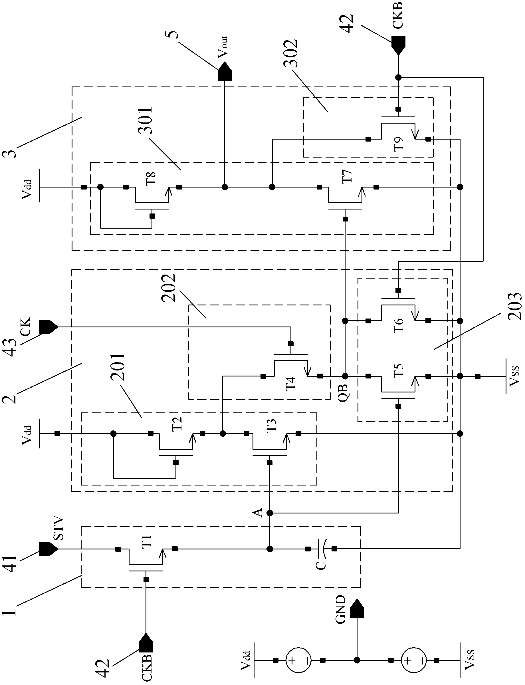
[0066] Such as figure 2 As shown, in a specific embodiment of the shift register unit circuit of the present invention, the switches T1 to T7 in this embodiment are all TFTs (Thin Film Transistors). It can be seen from the figure that the precharge circuit 1 is composed of a first switch T1, a first node A and a capacitor C; for the first switch T1, the gate is connected to the first clock signal CKB, and the drain is connected. The start signal (the start signal can be an STV signal, or a level signal output by the previous shift register unit circuit), the source is coupled to the first node A; the first node A is The pre-charging circuit 1 conducts the level output terminal; one end of the capacitor C is coupled to the first node A, and the other end is connected to the low level V SS .

[0067] The first level pull-down circuit 2 is composed of a first reverse circuit 201, a level pull-up circuit 202, and a first level pull-down sub-circuit 203. The first reverse circuit i...

Embodiment 2

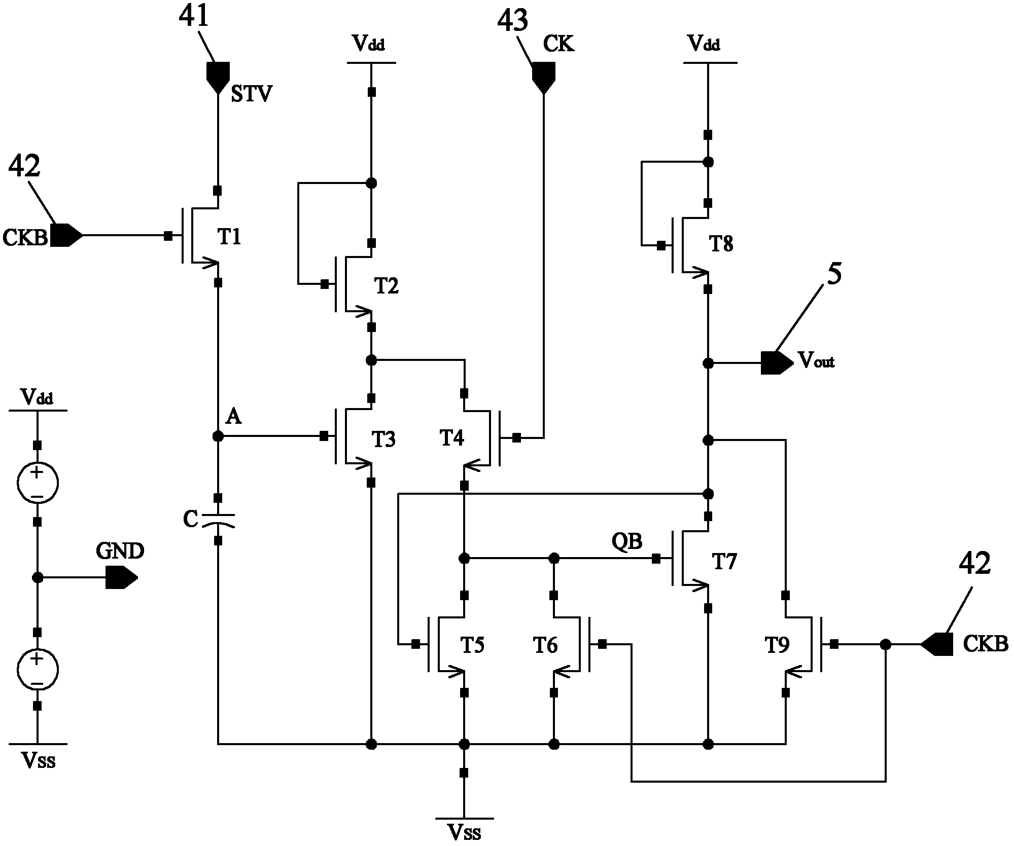
[0079] Such as image 3 As shown, another specific embodiment of the shift register unit circuit of the present invention, this embodiment only changes the gate of the fifth switch T5 in Embodiment 1 to be coupled to the second level pull-down circuit The output terminal of node A is the same as the output terminal V after t2. out The effect of the waveform on T5 is the same, that is, the working principle of this embodiment is the same as that of Embodiment 1.

[0080] Such as Figure 5 As shown, the shift register of the present invention includes a multi-stage shift register unit S 1 , S 2 ...S n , Each level of shift register unit is at the output terminal (OUT 0 , OUT 1 , OUT 2 ...OUT n ) Generate scan signals. Each level of shift register unit is equipped with a first clock access port CKB, a second clock access port CK, a start signal access port, a reset signal access port RT, and a scan signal output port OUT n . Each level of shift register unit circuit adopts the shi...


PUM


Abstract

The invention discloses a shift register unit circuit, a shift register and a liquid crystal display array substrate which are mainly designed for solving the problem of poor reliability of the existing shift register. The shift register provided by the invention comprises at least two shift register unit circuits in cascade connection, wherein each shift register unit circuit works based on two clock signals; and the unit circuit comprises an input end, a pre-charging circuit, a first level pull-down circuit, a second level pull-down circuit and an output end. By utilizing the shift register unit circuit and the shift register, the problem of drifting of the pull-down TFT (Thin Film Transistor) threshold voltage under direct-current bias voltage is solved, and simultaneously, the problem of unsteady output caused by clock transition is solved, the reliability of the circuit is improved, and the power consumption is reduced.

Description

Technical field [0001] The invention relates to the technical field of liquid crystal display, in particular to a shift register unit circuit, a shift register, an array substrate and a liquid crystal display. Background technique [0002] Liquid crystal display is a kind of flat display made of glass substrate. In order to pass the GOA circuit design (such as figure 1 The shown schematic diagram of the GOA circuit shift register unit circuit) adopts a manufacturing process for forming a TFT (Thin Film Transistor) in the pixel circuit, and integrates the driving circuit of the pixel circuit and the pixel circuit. In this case, in order to reduce manufacturing costs, it is better to use transistors of the same different electrical type for TFTs to form a drive circuit including a shift register. However, in the prior art, the shift register unit circuit formed by transistors of the same different electrical type of the TFT has problems such as the threshold voltage of the pull-do...

Claims


Application Information

Patent Timeline
Patent Type & Authority Applications(China)
IPC IPC(8): G09G3/36G09G3/20
CPCG09G3/3677G09G2300/0408G09G2310/0286G11C19/184G11C19/28
Inventor 李天马祁小敬青海刚
Owner BOE TECH GRP CO LTD
Why Eureka
Try Eureka