TFT (thin film transistor) array substrate as well as production method and manufacturing equipment for same

An array substrate, substrate technology, applied in its manufacturing method and manufacturing equipment, TFT-LCD array substrate field, can solve the problems of uneven polysilicon, Ioff increase, increase process cost and difficulty, etc.

Inactive Publication Date: 2012-09-05
BEIJING BOE OPTOELECTRONCIS TECH CO LTD
View PDF3 Cites 11 Cited by
  • Summary
  • Abstract
  • Description
  • Claims
  • Application Information

AI Technical Summary

Problems solved by technology

Therefore, it is necessary to use special technology to produce low-temperature polysilicon. One way is to deposit low-temperature polysilicon at a lower temperature, but this method requires expensive laser annealing equipment, and the polysilicon produced is not uniform.
Another way is to generate low-temperature polysilicon by the metal induction method, but this method requires an additional sputtering metal induction layer, and will introduce metal impurities into the polysilicon, resulting in an increase in Ioff
In addition, another disadvantage of using polysilicon is the need to increase the number of masks, increasing the cost and difficulty of the process

Method used


Image

  • TFT (thin film transistor) array substrate as well as production method and manufacturing equipment for same
  • TFT (thin film transistor) array substrate as well as production method and manufacturing equipment for same
  • TFT (thin film transistor) array substrate as well as production method and manufacturing equipment for same

Examples


Embodiment Construction

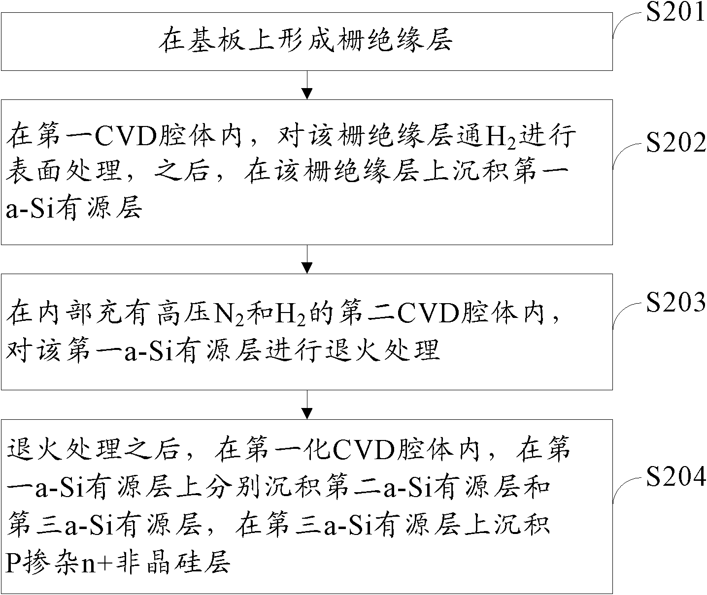
[0027] The following will clearly and completely describe the technical solutions in the embodiments of the present invention with reference to the accompanying drawings in the embodiments of the present invention. Obviously, the described embodiments are only some, not all, embodiments of the present invention. Based on the embodiments of the present invention, all other embodiments obtained by persons of ordinary skill in the art without making creative efforts belong to the protection scope of the present invention.

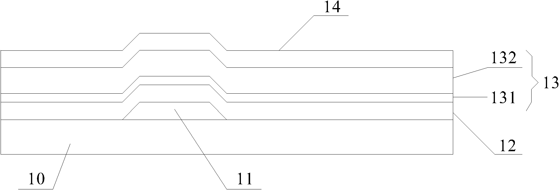
[0028] In the existing technology, such as figure 1 As shown, after the gate 11 is formed on the substrate 10 , a gate insulating layer 12 , an a-Si (amorphous silicon) active layer 13 and a P-doped n+ amorphous silicon layer 14 are deposited on the substrate 10 . The deposition of the gate insulating layer 12 , the a-Si active layer 13 and the P-doped n+ amorphous silicon layer 14 is collectively referred to as CVD (Chemical Vapor Deposition, chemical vapor d...


PUM


Abstract

The embodiment of the invention provides a TFT (thin film transistor) array substrate as well as a production method and manufacturing equipment for the same, relating to the field of manufacturing for thin-film-transistor liquid crystal displayer, being capable of improving the charge characteristic of TFT and increasing the carrier mobility of TFT, as well as being simple and convenient in realization, and low in cost. The method comprises the following steps of: forming a gate insulating layer on a substrate; charging H2 to perform surface treatment on the gate insulating layer in a first CVD (chemical vapour deposition) cavity, and then depositing a first a-Si active layer on the gate insulating layer; performing annealing treatment on the first a-Si active layer in a second CVD cavity internally charged with high-pressure N2 and H2; and after the annealing treatment, depositing a second a-Si active layer and a third a-Si active layer on the first a-Si active layer respectively, and depositing a P-doped n<+> amorphous silicon layer on the third a-Si active layer in the first CVD cavity. The method provided by the embodiment of the invention is used for manufacturing a TFT array substrate.

Description

technical field [0001] The invention relates to the field of manufacturing thin film transistor liquid crystal displays, in particular to a TFT-LCD array substrate, a manufacturing method and manufacturing equipment thereof. Background technique [0002] TFT-LCD (Thin Film Transistor-Liquid Crystal Display, Thin Film Transistor-Liquid Crystal Display) uses the change of the electric field intensity sandwiched on the liquid crystal layer to change the orientation of liquid crystal molecules, thereby controlling the intensity of light transmission to display images. Generally speaking, a complete liquid crystal display panel must have a backlight module, a polarizer, a TFT lower substrate, a CF (color filter) upper substrate, and a liquid crystal molecule layer filled in a box composed of these two substrates. There are a large number of pixel electrodes on the TFT substrate, and the on-off and magnitude of the voltage on the pixel electrodes are controlled by the gate connect...

Claims


Application Information

Patent Timeline
Patent Type & Authority Applications(China)
IPC IPC(8): H01L21/77H01L27/12H01L21/20
Inventor 张金中
Owner BEIJING BOE OPTOELECTRONCIS TECH CO LTD
Why Eureka
Try Eureka