Organic thin film transistor and manufacturing method thereof

An organic thin film and manufacturing method technology, which is applied in semiconductor/solid state device manufacturing, electric solid state device, semiconductor device and other directions, can solve the problems of increased manufacturing cost, complex process and many processing steps of organic thin film transistors, and achieves simplified manufacturing process, Reduce manufacturing costs, overcome the effects of complex patterning methods

Inactive Publication Date: 2012-09-05
BOE TECH GRP CO LTD
View PDF5 Cites 2 Cited by
  • Summary
  • Abstract
  • Description
  • Claims
  • Application Information

AI Technical Summary

Problems solved by technology

[0007] Embodiments of the present invention provide an organic thin film transistor and a manufacturing method thereof, which can solve the problem that the manufacturing cost of the organic thin film transistor is increased due to complex processes and many processing steps in the manufacturing process of the organic thin film transistor with a top-gate top-contact electrode structure. question

Method used


Image

  • Organic thin film transistor and manufacturing method thereof
  • Organic thin film transistor and manufacturing method thereof
  • Organic thin film transistor and manufacturing method thereof

Examples


Embodiment 1

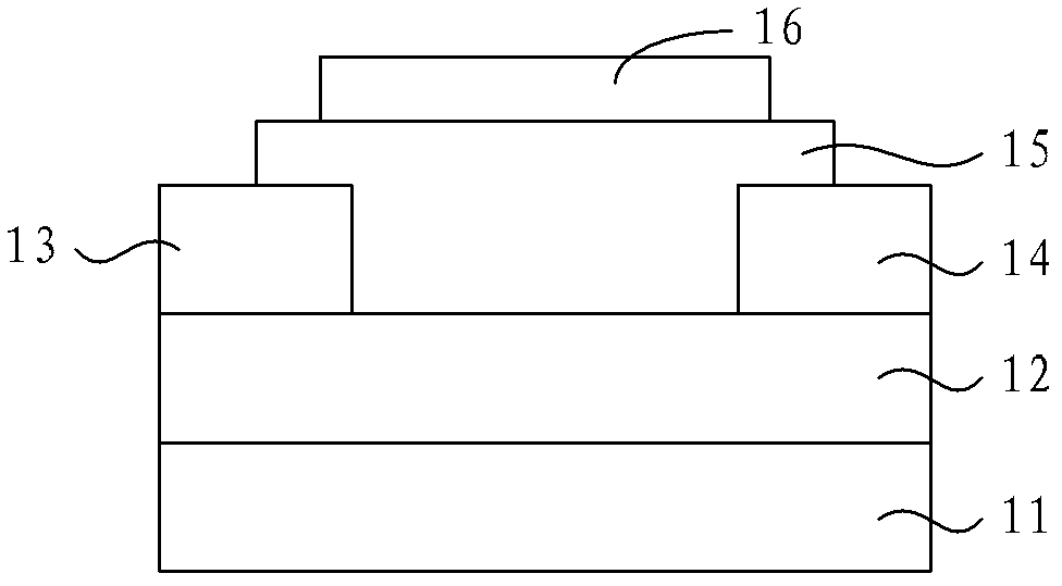
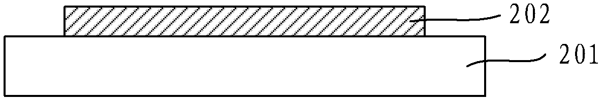
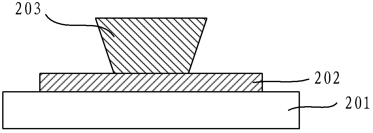
[0023] This embodiment provides an organic thin film transistor, such as Figure 2C As shown, the organic thin film transistor includes: a substrate 201 , an organic semiconductor layer 202 , a gate insulating layer 203 , a gate electrode 204 , a source electrode 205 and a drain electrode 206 . A gate insulating layer 203 is formed on the organic semiconductor layer 202; a gate electrode 204 covers the top surface of the gate insulating layer 203; a source electrode 205 and a drain electrode 206 are formed on the organic semiconductor layer 202, facing each other across the gate insulating layer 203, and respectively Close to the sidewall 207 of the gate insulating layer 203; the angle α between the sidewall 207 and the bottom surface of the source electrode 205 or the drain electrode 206 close to the sidewall is not greater than 90 degrees. Wherein, the material of the gate insulating layer 203 is a photosensitive material.

[0024] The manufacturing method of the above-ment...

Embodiment 2

[0038] This embodiment provides an organic thin film transistor, such as image 3 As shown, the organic thin film transistor includes: a substrate 301 , an organic semiconductor layer 302 , a gate insulating layer 303 , a gate electrode 304 , a source electrode 305 and a drain electrode 306 . A gate insulating layer 303 is formed on the organic semiconductor layer 302; a gate electrode 304 covers the top surface of the gate insulating layer 303; a source electrode 305 and a drain electrode 306 are formed on the organic semiconductor layer 302, facing each other across the gate insulating layer 303, and respectively Close to the sidewall 307 of the gate insulating layer 303; the angle between the sidewall 307 and the bottom surface of the source electrode 305 or the drain electrode 306 close to the sidewall is 90 degrees (that is, the sidewall 307 is perpendicular to the organic semiconductor layer 302 top surface). Wherein, the material of the gate insulating layer 303 is a p...


PUM


Abstract

The invention discloses an organic thin film transistor and a manufacturing method thereof, and relates to the field of organic semiconductor devices. The manufacturing method provided by the invention comprises the following steps of: forming an organic semiconductor layer on a substrate, forming a grid insulating layer made of photosensitive material on the organic semiconductor layer, and carrying out exposure on the grid insulating layer; carrying out developing on the grid insulating layer after exposure to obtain the grid insulating layer with a pattern; and forming a metal film on the organic semiconductor layer which can form the grid insulating layer with the pattern, namely, forming a gate electrode covering the top surface of the grid insulating layer, and forming a source electrode and a leakage pole which are opposite to each other across the grid insulating layer and respectively closely prop against the side wall of the grid insulating layer. The organic thin film transistor and the manufacturing method thereof provided by the invention have the advantages of simplifying the manufacturing process of the organic thin film transistor, and reducing the manufacturing cost of the organic thin film transistor.

Description

technical field [0001] The invention relates to the field of organic semiconductor devices, in particular to an organic thin film transistor and a manufacturing method thereof. Background technique [0002] Organic Thin-film Transistors (abbreviated as: OTFT) is a field-effect device with logic switching characteristics that uses an organic semiconductor as an active layer. Compared with thin-film transistors (Thin-film Transistors, TFT for short) of traditional silicon materials, organic thin-film transistors have significant advantages of low-temperature processing, light weight, large-area integration, and compatibility with flexible substrates. [0003] According to the position of the gate electrode, the organic thin film transistor can be divided into a bottom gate structure and a top gate structure, and according to the position sequence of the source / drain electrode and the active layer, the organic thin film transistor can also be divided into a bottom contact elect...

Claims


Application Information

Patent Timeline
Patent Type & Authority Applications(China)
IPC IPC(8): H01L51/05H01L51/10H01L51/40
Inventor 张学辉
Owner BOE TECH GRP CO LTD
Why Eureka
Try Eureka