Ultrahigh voltage BCD (Bipolar CMOS DMOS) process and ultrahigh voltage BCD device

An ultra-high voltage, semiconductor technology, applied in the direction of semiconductor devices, semiconductor/solid-state device manufacturing, electric solid-state devices, etc.

Active Publication Date: 2012-09-12
ADVANCED SEMICON MFG CO LTD
View PDF4 Cites 27 Cited by
  • Summary
  • Abstract
  • Description
  • Claims
  • Application Information

AI Technical Summary

Problems solved by technology

[0005] The technical problem to be solved by the present invention is to provide an ultra-high voltage BCD semiconductor process and a device realized by the ultra-high voltage BCD process to solve the integration problem of various voltage level devices

Method used


Image

  • Ultrahigh voltage BCD (Bipolar CMOS DMOS) process and ultrahigh voltage BCD device
  • Ultrahigh voltage BCD (Bipolar CMOS DMOS) process and ultrahigh voltage BCD device
  • Ultrahigh voltage BCD (Bipolar CMOS DMOS) process and ultrahigh voltage BCD device

Examples


Embodiment Construction

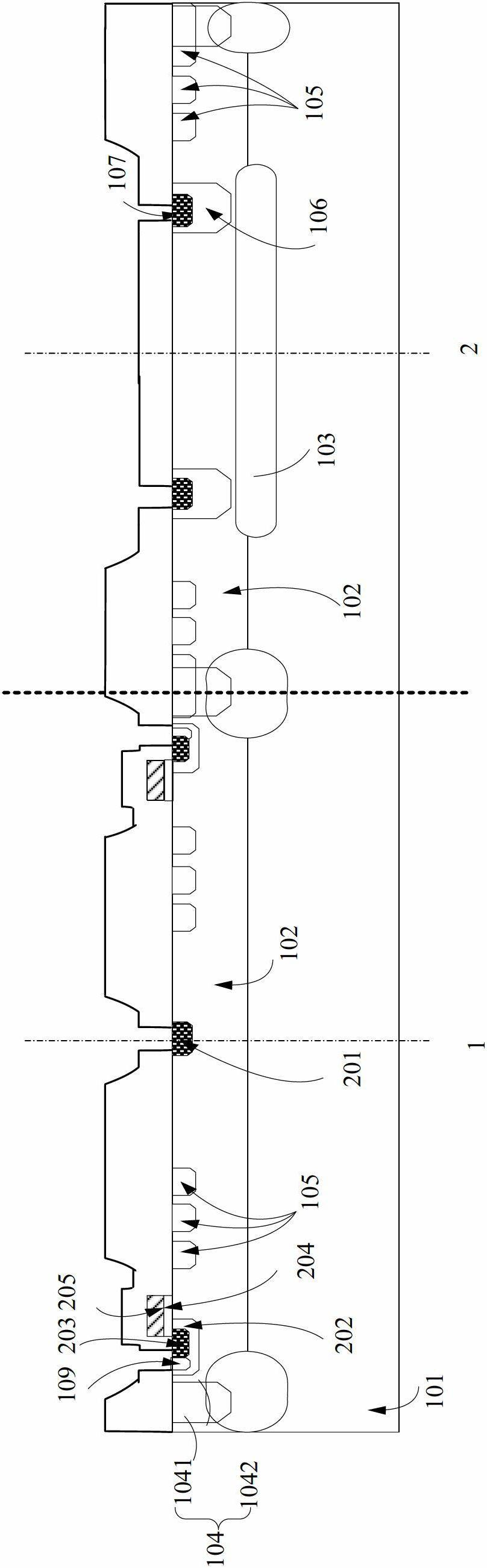
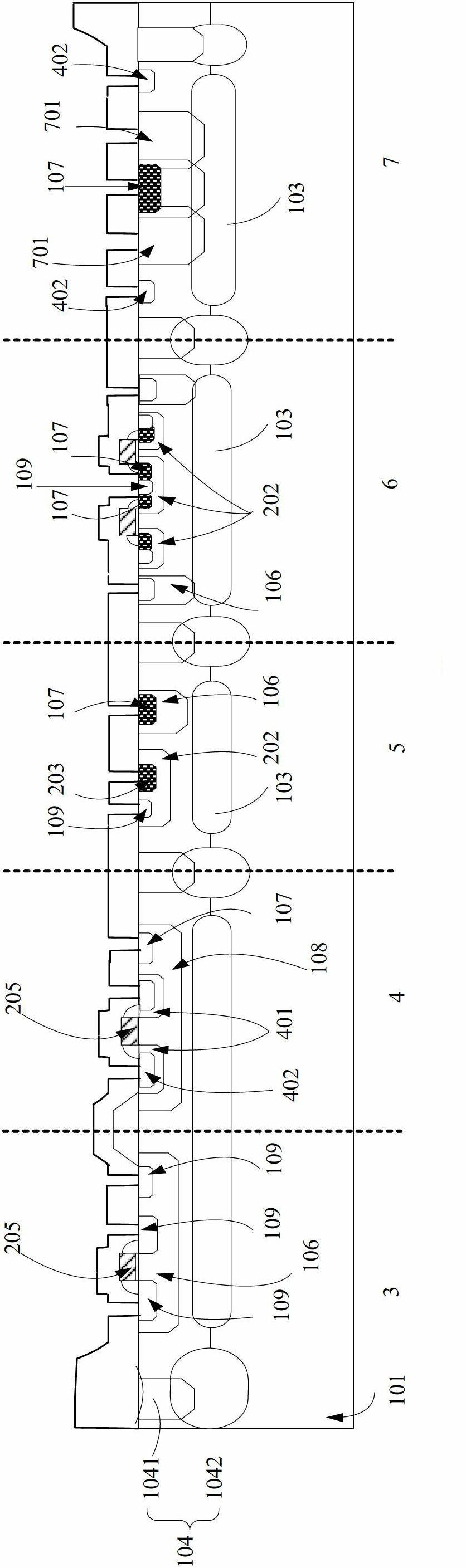
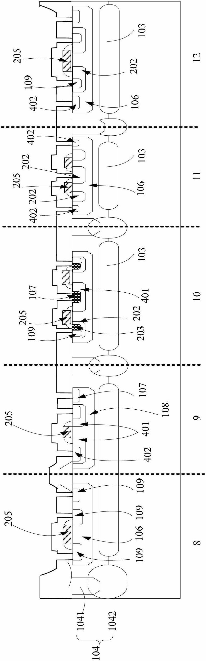
[0028] An ultra-high voltage BCD semiconductor device and an ultra-high voltage BCD process proposed by the present invention will be further described in detail below with reference to the drawings and specific embodiments. Advantages and features of the present invention will be apparent from the following description and claims. It should be noted that all the drawings are in very simplified form and use imprecise ratios, which are only used for the purpose of conveniently and clearly assisting in describing the embodiments of the present invention.

[0029] The core idea of ​​the present invention is that the ultra-high voltage BCD semiconductor device provided by the present invention includes devices of various voltage levels, and the high-voltage floating basin structure can provide process platform support for the application of bridge circuits; the ultra-high voltage BCD semiconductor device provided by the present invention High-voltage BCD process, which adopts the ...


PUM


Abstract

The invention provides an ultrahigh voltage BCD process which can be used for realizing integration of a plurality of semiconductor devices. An ultrahigh voltage BCD device comprises a high-voltage LDMOS (Laterally Diffused Metal Oxide Semiconductor) manufactured on an N-type extension, a high-voltage floating tub structure, a low-voltage PMOS (P-channel Metal Oxide Semiconductor) transistor, a low-voltage NMOS (N-channel Metal Oxide Semiconductor) transistor, a low-voltage VNPN transistor, a VDNMOS, a Zener diode, a low-voltage NLDMOS, an LPNP, and a symmetrical drain extension EDPMOS. The process has an N-type buried layer which penetrates through a P-type substrate and an N-type extension, a PN junction through isolation structure is formed between the high-voltage structure and the low-voltage structure. The high-voltage BCD process integrates devices of a plurality of voltage levels, wherein the high-voltage floating tub structure can provide process platform support for application of a bridge type circuit.

Description

technical field [0001] The invention relates to the field of semiconductor manufacturing technology, in particular to an ultra-high voltage BCD semiconductor technology and an ultra-high voltage BCD device. Background technique [0002] BCD is a monolithic integration process technology that can make bipolar transistors (Bipolar Junction Transistor), CMOS and DMOS devices on the same chip. The BCD process not only combines the advantages of high transconductance, strong load driving capability of bipolar devices, high integration and low power consumption of CMOS, but also integrates high withstand voltage DMOS power devices. Since DMOS has the characteristics of high-voltage and high-speed switching at the same time, the power management chip manufactured by BCD process can work at high voltage and high frequency, which is an ideal process for manufacturing high-performance power chip. The monolithic integrated chip manufactured by the BCD process can improve system perfor...

Claims


Application Information

Patent Timeline
Patent Type & Authority Applications(China)
IPC IPC(8): H01L27/06H01L21/8249
Inventor 吕宇强邵凯陈雪萌杨海波
Owner ADVANCED SEMICON MFG CO LTD
Why Eureka
Try Eureka