Optical element, optical element module, electronic element module, and electronic information device
A technology of optical components and electronic components, applied in the direction of optical components, optical, electrical components, etc., can solve problems such as ghosting and flare
- Summary
- Abstract
- Description
- Claims
- Application Information
AI Technical Summary
Problems solved by technology
Method used
Image
Examples
Embodiment 1)
[0090] figure 1is a perspective view for briefly describing a method of manufacturing a lens wafer module according to Embodiment 1 of the present invention. figure 1 (a) is a perspective view schematically showing two lens wafers and a light-shielding plate therebetween before lamination. figure 1 (b) is a perspective view schematically showing the lens wafer module after lamination.
[0091] Such as figure 1 As shown in (a), initially, two lens wafers 11 and 12 on the top and bottom are provided as an optical element wafer having a plurality of lenses arranged in a two-dimensional matrix pattern, and light shielding plates 13 are provided on the top and bottom Between the two lens wafers 11 and 12, openings therein for each lens are formed in a matrix pattern. Next, the positions of the lenses 11 a , 12 a and the opening 13 a are aligned such that the positions of the lenses 11 a and 12 a of the respective lens wafers 11 and 12 are aligned with the positions of the op...
Embodiment 2)
[0105] In Embodiment 1, the case of a wafer-level process, or specifically, the case of obtaining a plurality of lens modules 1 by cutting the lens wafer module 10 modularized using a plurality of lens wafers, was described. However, in Embodiment 2, the case of the injection molding process, specifically, the case of manufacturing a single lens by the injection molding process will be described.
[0106] Figure 5 (a) is a longitudinal sectional view schematically showing a lens manufactured by an injection molding process as an optical element of Example 2 of the present invention. Figure 5 (b) is Figure 5 (a) Rear view of the lens. Figure 6 (a) is used to describe Figure 5 (a) Longitudinal cross-sectional view of the lens fabrication method. Figure 6 (b) is Figure 6 (a) Rear view of the lens.
[0107] Such as Figure 5 As shown in (a) and 5(b), the lens 20 as the optical element of Embodiment 2 is formed by resin injection molding using a material such as a trans...
Embodiment 3)
[0111] In Embodiment 1, the lens module 1 is obtained by dicing the lens wafer module 10 manufactured by a wafer-level process. In Example 2, a lens 20 manufactured by an injection molding process was obtained. In Embodiment 3, an imaging module using the lens module 1 or the lens 20 according to Embodiments 1 and 2, respectively, will be described.
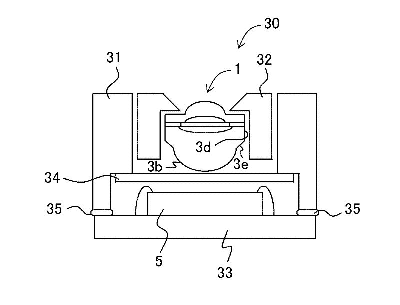
[0112] Figure 7 is a longitudinal sectional view schematically showing an imaging module according to Embodiment 3 of the present invention.
[0113] exist Figure 7 Among them, the imaging module 30 as the electronic component module of Embodiment 3 includes: a holder 31 as a dust cover; a lens holder 32 installed on the upper part of the holder 31; a condenser lens module accommodated in the lens holder 32 1 (or lens 20 ); substrate 33 ; solid-state imaging element 5 (sensor chip) as an electronic component, provided on substrate 33 and wire-bonded to substrate 33 ; IR cut filter 34 , fixed to a stepped portion inside holde...
PUM
 Abstract
Description
Claims
Application Information


