
LED (Light Emitting Diode) integrated packaging substrate with shortest bonding wire and light source module applying substrate

An integrated packaging and substrate technology, applied in the direction of electrical components, circuits, semiconductor devices, etc., can solve the problems of uneven light output, difficulty, and large light loss of the light source, and achieve the benefits of optical design, improve light output efficiency, and increase light output rate. Effect

Active Publication Date: 2012-09-19
FOSHAN EVERCORE OPTOELECTRONICS TECH
View PDF1 Cites 3 Cited by
  • Summary
  • Abstract
  • Description
  • Claims
  • Application Information

AI Technical Summary

Problems solved by technology

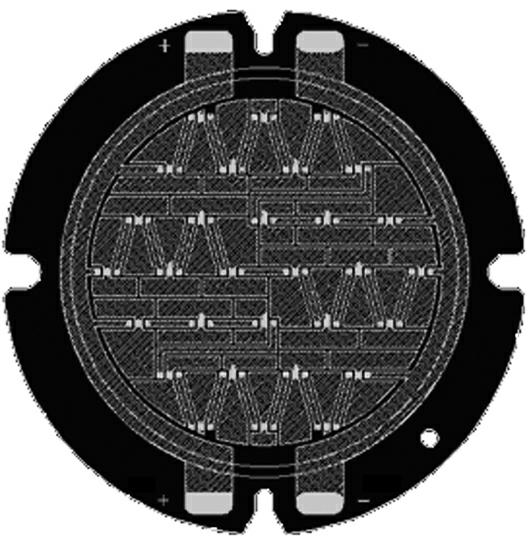
[0005] The circuit of the traditional LED integrated packaging substrate is generally formed by parallel matrix wiring or a combination of parallel wiring and oblique lines, such as figure 1 As shown, this routing method has limitations on the placement of the light source chip. Often, the entire light source will emit uneven light due to unreasonable placement of the chip, excessive light loss due to the placement of the chip, and excessive light loss due to the placement of the chip. If placed far away, the light will be blocked by too long bonding wires, the light will be damaged due to too long wires, or the circuit design will be difficult, difficult to process or difficult to pass safety inspections, etc.
[0006] The circuit of traditional LED integrated packaging substrates is generally composed of parallel symmetrical matrix wiring or a combination of parallel wiring and oblique lines. This wiring method has limitations on the structure of the chip. The chip is generally divided into horizontal structure and vertical structure. , when using traditional packaging substrates for integration and combination, if it is necessary to use vertical structure chips and horizontal structure chips for combined packaging at the same time, it will be difficult, because it cannot be realized due to the complicated wiring, or it cannot pass the safety inspection

Method used


Image

  • LED (Light Emitting Diode) integrated packaging substrate with shortest bonding wire and light source module applying substrate
  • LED (Light Emitting Diode) integrated packaging substrate with shortest bonding wire and light source module applying substrate
  • LED (Light Emitting Diode) integrated packaging substrate with shortest bonding wire and light source module applying substrate

Examples


Embodiment 1

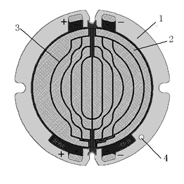
[0030] refer to figure 2 , the LED integrated packaging substrate with the shortest bonding wire in the present invention includes a substrate main body, a common circuit arranged on the substrate main body, and a die-bonding area 2 arranged on the substrate main body, and the die-bonding area 2 is divided into at least two In the integrated area, the public circuit is an integrated metal plate and is arranged correspondingly to the integrated area. Each integrated area corresponds to a common circuit. The common circuits are insulated from each other and have opposite electrodes. The integrated metal plate forms a circuit area. The entire metal plate can be used as the lead pad of the LED chip; any position in the area of ​​the integrated die-bonding area can be used as the bonding position of the LED chip; the integrated die-bonding area can be formed by a circle, a line segment or a Surrounded by any combination of solitary and line segments, the integrated die bonding are...

Embodiment 2

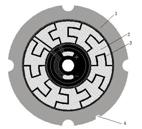
[0035] refer to image 3 , The difference between this embodiment and Embodiment 1 is that the area surrounding the die bonding is surrounded by broken lines, and the fool-proof holes 4 are set as fool-proof grooves.


PUM


Abstract

The invention discloses an LED (Light Emitting Diode) integrated packaging substrate which comprises a substrate main body, common circuits arranged on the substrate main body, and a die bonding section arranged on the substrate main body. The die bonding section is divided into at least two integral areas, every two adjacent areas are mutually insulated and the electrodes of every two adjacent areas are opposite. The common circuits are an integral metal plate and are arranged in correspondence with the integral areas, and the common circuits are mutually insulated. One electrode lead of an LED chip is bonded in the die bonding area in which the LED chip is arranged and the other electrode lead is bonded in the die bonding area adjacent to the die bonding area in which the chip is arranged, and is connected with the common circuits. The two electrode leads of the LED chip can be bonded at the nearest sites at the corresponding areas, and in such a way, the bonding wire is the shortest.

Description

technical field [0001] The invention relates to the technical field of LED lighting and the field of LED packaging, in particular to an LED integrated packaging substrate with the shortest bonding wire and a light source module using the substrate. Background technique [0002] As a new type of light source, LED has the characteristics of environmental protection and energy saving, high brightness, long life, fast start-up speed, and high chroma. It is widely used in outdoor advertising displays, indoor lighting, decorative lights, and emergency lights. [0003] Since the 1990s, many breakthroughs have been made in the research and development of LED chip and material manufacturing technology, which has made epitaxial wafer and chip technology increasingly mature. At the same time, the improvement of LED chip efficiency and the expansion of LED application technology have also changed the existing LED packaging. Technology has transformed the mainstream LED packaging technol...

Claims


Application Information

Patent Timeline
Patent Type & Authority Applications(China)
IPC IPC(8): H01L33/48H01L33/62
Inventor 王孟源
Owner FOSHAN EVERCORE OPTOELECTRONICS TECH
Learn More