Multi-channel parallel optical component for high-speed transmission and assembly method thereof

A technology of high-speed transmission and optical components, applied in the coupling of optical waveguides, etc., can solve problems such as signal transmission distortion and affect communication quality, and achieve the effects of improving capabilities, avoiding parasitic capacitance and inductance, and reducing the length of gold wires

Inactive Publication Date: 2016-08-24
昆山柯斯美光电有限公司
View PDF5 Cites 0 Cited by
  • Summary
  • Abstract
  • Description
  • Claims
  • Application Information

AI Technical Summary

Problems solved by technology

Due to the limitation of PCB board manufacturing technology (usually the line width and line spacing is 4mil / 4mil) and the radian higher than the PCB board wiring, etc., it is often made from the driver circuit chipset to the VCSEL chip array or / and PD chip array and PCB. The wiring distance of the circuit lines on the board exceeds 1mm, and the 40G / 100G transmission signal requires that the wiring length should not exceed 1mm, otherwise some parasitic capacitance and inductance will easily occur, which will cause signal distortion during transmission and affect communication quality.
And mount the driving circuit chipset and the corresponding VCSEL chip array or / and PD chip array on the chip carrier (PCB board), and the heat generated by the 40G / 100G transmission signal comes from the driving circuit chipset array and the photoelectric chip array group , there is a problem of chip heat dissipation

Method used


Image

  • Multi-channel parallel optical component for high-speed transmission and assembly method thereof
  • Multi-channel parallel optical component for high-speed transmission and assembly method thereof
  • Multi-channel parallel optical component for high-speed transmission and assembly method thereof

Examples


Embodiment Construction

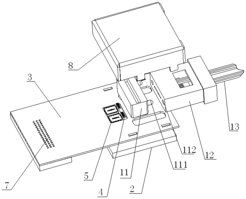
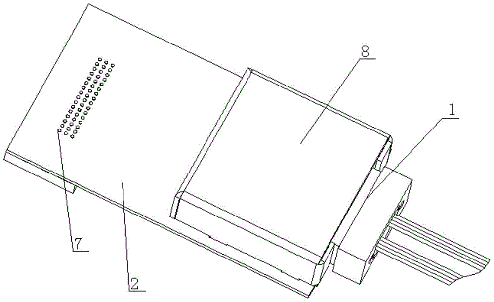
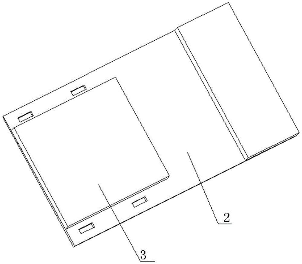
[0039] Such as figure 1 , figure 2 , image 3 , Figure 4 , Figure 5 and Figure 6 As shown, a multi-channel parallel optical assembly for high-speed transmission includes a parallel optical fiber coupling alignment assembly 1, a backing board 2, a chip carrier 3 (PCB flexible board or hard board), an optoelectronic chip array group 4 (such as a VCSEL chip array or / and PD chip array) and a drive circuit chipset 5 for driving the photoelectric chip array group; the photoelectric chip array group is mounted on the substrate, and the drive circuit chipset is close to the photoelectric One side of the chip array group is mounted on the substrate; the middle part of the chip carrier has a through hole 31 that matches the shape and size of the drive circuit chip group and the optoelectronic chip array group after mounting; The chip carrier is mounted on the backing board, and the photoelectric chip array group and the driving circuit chip group are penetrated in the through h...


PUM


Abstract

The invention discloses a multi-path parallel optical component for high-speed transmission and the assembling method thereof. The optical component comprises a parallel optical fiber coupling and aligning component, a lining plate, a chip carrier, a photoelectric chip array set and a driving circuit chip set, wherein the photoelectric chip array set is attached to the lining plate, the driving circuit chip set is attached to the lining plate, a through hole is formed in the middle of the chip carrier, the chip carrier is attached to the lining plate, the photoelectric chip array set and the driving circuit chip set are made to be arranged in the through hole in a penetrating mode, and the thickness difference between the driving circuit chip set and the chip carrier is preset; the driving circuit chip set is connected with the photoelectric chip array set and a circuit wire on the periphery of the through hole in the chip carrier in a routing mode, and the photoelectric chip array set is coupled and aligned with the parallel optical fiber coupling and aligning component. According to the multi-path parallel optical component, the routing length between the driving circuit chip set and the photoelectric chip array set and the routing length between the driving circuit chip set and the circuit wire on the chip carrier can be reduced, parasitic inductance and capacitance generated by routing are reduced greatly, and the high-speed signal transmission capacity is improved.

Description

technical field [0001] The invention relates to the technical field of optical fiber communication, in particular to a multi-channel parallel optical component for high-speed transmission and an assembly method thereof. Background technique [0002] In order to meet people's increasing demand for communication bandwidth, increasing transmission capacity and reducing power consumption are the top priorities in the field of optical fiber communication, and parallel optical fiber technology is thus increasingly developed. At present, the main products using parallel optical fiber technology include QSFP optical modules, CFP optical modules, Thunderbolt cables, optical active HDMI cables, etc. The main feature of parallel optics technology is multiple parallel lasers or parallel photodiodes aligned with multiple optical fibers in a single device or module. Multi-channel parallel optical components or modules for high-speed transmission usually include multiple parallel laser ar...

Claims


Application Information

Patent Timeline
Patent Type & Authority Patents(China)
IPC IPC(8): G02B6/43
Inventor 刘维伟邵乾刘洪波刘让陈曦蒋维楠蒋文斌
Owner 昆山柯斯美光电有限公司
Why Eureka
Try Eureka