Approach to the manufacturing of monolithic 3-dimensional high-rise integrated-circuits with vertically-stacked double-sided fully-depleted silicon-on-insulator transistors

a technology of silicon-on-insulator transistors and integrated circuits, which is applied in the direction of semiconductor devices, semiconductor/solid-state device details, electrical apparatus, etc., can solve the problems of limiting volume of tsvs, and achieve the optimization of power consumption for given performance, reduce parasitic power consumption, and reduce on-state performance

Active Publication Date: 2020-02-11
TARAKJI AHMAD +1
View PDF20 Cites 1 Cited by
  • Summary
  • Abstract
  • Description
  • Claims
  • Application Information

AI Technical Summary

Benefits of technology

[0007]After the 90 nm CMOS technology node the RC delays from the inline interconnects have become substantially pronounced to dominate the speed of Central-Processing-units (CPUs). In today's most advanced systems these RC delays are already two to four orders of magnitude higher than the device Gate delays. This is negating in the first place all and any performance enhancements from the Frontend. Furthermore it is well known that the inline interconnects alone in these technology nodes are accounting to more than 50% of the dynamic dissipated total power in processors. Because of these, any and all progress to the performance and to the power-efficiency of microprocessors, microcontrollers and most ICs has become largely dependent today on reducing RC delays and the parasitic power consumed in inline interconnects. This invention reduces the lengths, the impedances and the RC delays of interconnects that wire the different discrete transistors in monolithic Three-Dimensional Integrated-Circuits (3D-ICs); it therefore eliminates or substantially reduces the much longer wirings that interconnect the transistors in today's modern CPUs. It also allows very dense interconnections to be realized between the discrete devices or transistors in same 3D-ICs. The vertical wiring of transistors will no longer require the thick, bulky and “difficult to manufacture” through-Silicon-Vias (TSVs) that some prior art is using today. These thick bulky TSVs do limit the volume to vertically integrate the transistors. This invention rather comprises discrete ultra-thinned (3-100 nm) semiconductor (e.g. silicon) films embodying transistor structures that are fully submerged and dispersed in thick inline dielectric. The invention is distinctly unique in that these discrete transistors are optimally positioned one on top another and are interconnected or inter-wired inside this dielectric in Three-Dimensional configurations. Transistors no longer need to interconnect by climbing many higher Metal layers and tumbling down, like in today's CPUs, they will rather interconnect laterally and on top of one another in fully monolithic Three-Dimensional integrations. The invention is peculiar in its innovative new architecture that enables interconnects to contact the Drain and Source of a transistor at more than one surface of its semiconductor film wherein these Drain and Source regions overlap the many surfaces of this transistor that are exposed to the inline dielectric. This enables a transistor in one semiconductor film to connect to other transistor in different semiconductor film with much shorter wiring(s). Same invention also encompasses dual-gate MOSFET designs that make use of secondary fully independent Gate that intelligently fine-tunes in real-time the device threshold-voltage while all the primary Gates of devices are affixed or tied to their Logic or Memory circuits. A Gate of one transistor can connect to a Gate of another transistor that is embodied in different semiconductor film via shortest cut that minimizes the length of this wiring. Ultra-thinned sheets of semiconductor (e.g. silicon) incorporating a one Gate with its corresponding insulating dielectric on each of the two surface sides of this ultra-thinned semiconductor form this dual-gate MOSFET. Its Gates work-functions are specially tailored to lower device threshold-voltage and provide good short-channel control for off-state leakage current.
[0008]In such dual-gate MOSFETs one Gate can or will assume the functionality of the Back-Gate in today's conventional Fully-Depleted Silicon-On-Insulator transistors and serves as a fully independent knob that can be software-programmed to intelligently boost or reduce the on-state performance (through automatically fine-tuning the device Threshold-Voltage) such to best optimize the power consumption for given performance. This does or will drastically reduce the parasitic power consumed in the standby modules and in Memories (e.g. in SRAM cells). It for example enables a Drone or an Areal-Vehicle-System (AVS) to intelligently fine-tune or alternate the mode of its operation for lowest consumed power when it is simply flying and for highest performance while it rapidly processes and analyzes areal images and / or detects and tracks given target(s). It can also serve to intelligently slow-down specific overheated modules (or subsystems) of an Integrated-Circuit (IC) temporarily till they get cooled-down instead of fully shutting them off during this cooling process.

Problems solved by technology

These thick bulky TSVs do limit the volume to vertically integrate the transistors.

Method used


Image

  • Approach to the manufacturing of monolithic 3-dimensional high-rise integrated-circuits with vertically-stacked double-sided fully-depleted silicon-on-insulator transistors
  • Approach to the manufacturing of monolithic 3-dimensional high-rise integrated-circuits with vertically-stacked double-sided fully-depleted silicon-on-insulator transistors
  • Approach to the manufacturing of monolithic 3-dimensional high-rise integrated-circuits with vertically-stacked double-sided fully-depleted silicon-on-insulator transistors

Examples


Embodiment Construction

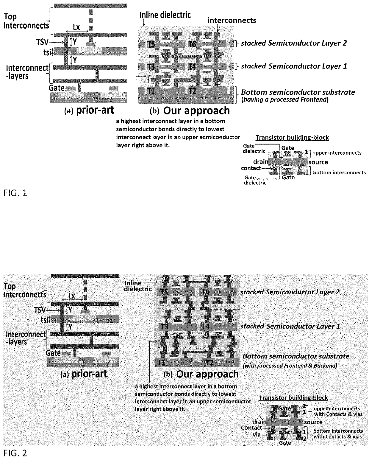
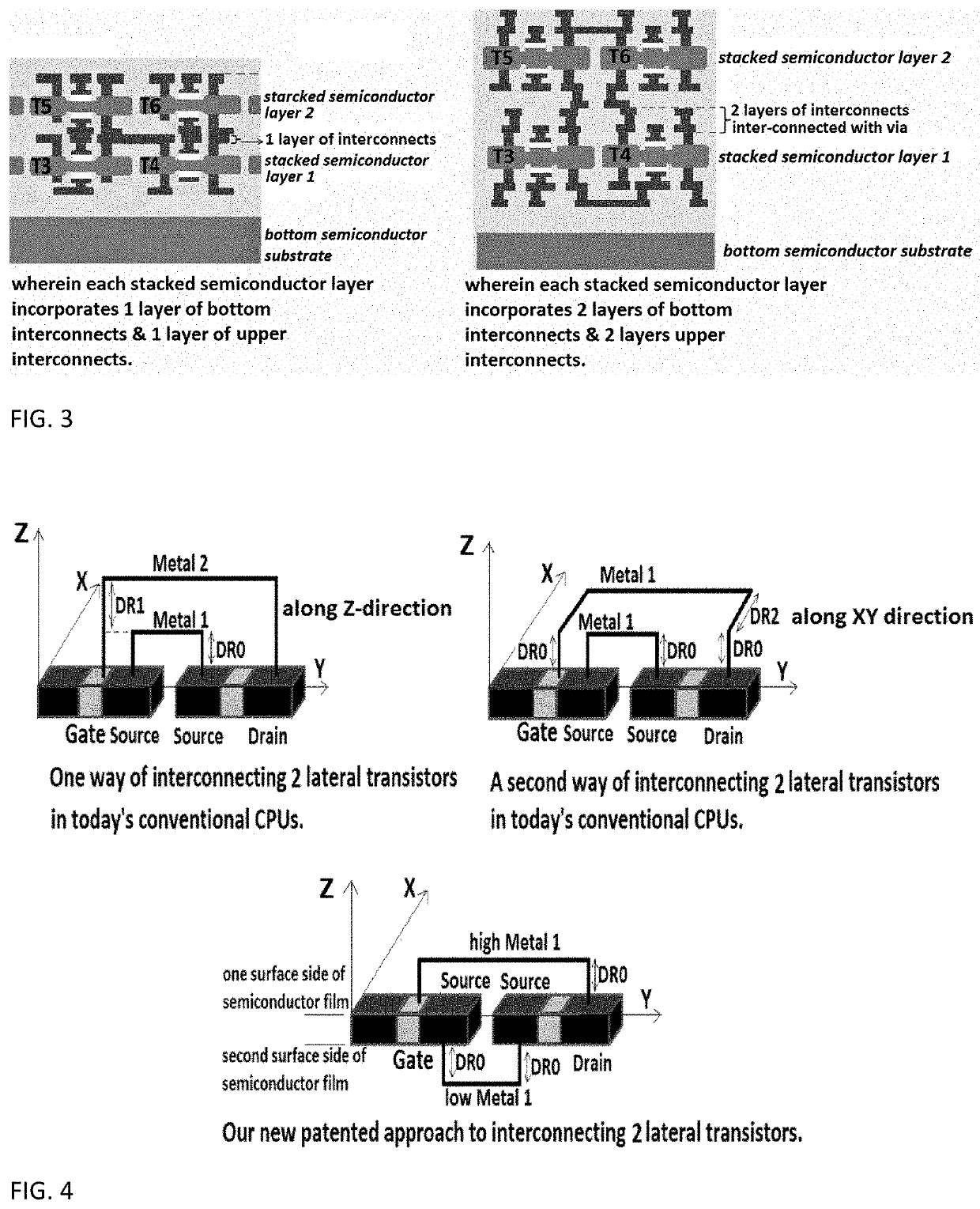
[0016]FIG. 1, FIG. 2 and FIG. 3 show a side-by-side comparison between the prior-art to monolithic 3D-ICs that is being considered and evaluated today, and our new-approach that eliminates the TSVs. Our new-approach is shown to include four transistors: T1, T2, T3, and T4, wired to each other in a dielectric through inline interconnects. The transistor's Drain and Source regions in our new-approach to monolithic 3D-IC architecture encompass or cover the many surface sides of the thinned semiconductor films that are exposed to the inline dielectric. This enables a Drain or a Source of one transistor to contact the terminal(s) (Drain, Source, Gate) of another transistor with shortest possible path(s) and without having interconnect(s) go around either of the two transistors like in the case of prior-art which representative schematic is shown next to the representative schematic of our new-approach. This significantly reduces delays and power consumptions in interconnects. When dual-G...


PUM

PropertyMeasurementUnit
Gate lengthaaaaaaaaaa
thicknessaaaaaaaaaa
thicknessaaaaaaaaaa

Abstract

A new architecture to fabricate high-rise fully monolithic three-dimensional Integrated-Circuits (3D-ICs) is described. It has the major advantage over all known prior arts in that it substantially reduces RC-delays and fully eliminates or very substantially reduces the large and bulky electrically conductive Through-Silicon-VIAS in a monolithic 3D integration. This enables the 3D-ICs to have faster operational speed with denser device integration.

Description

BACKGROUND OF THE INVENTION[0001]As the Semiconductor industry is entering the era that foresees the end of miniaturization of the Silicon transistor, engineers are already considering newer approaches to boost the device density, the efficiency, and the performance of the logic and memory Chips without necessitating the move to smaller transistors. Although Three-Dimensional (3D) circuits are nothing new given that Integrated-Circuits (ICs) are routinely packaged nowadays one on top another via wire-bonds or large copper pillars called Through-Silicon-Via's (TSV's) that vertically connect the ICs together, the concept has still limitations. For one thing, these 3D-Packages are interconnecting the subsystems and not their discrete components. This is consequently limiting the density of 3D interconnections and the overall Chip performance. Further, even in substituting wire-bonds with TSV's the resulting effects from RC delays and higher impedances between subsystems were reported t...

Claims


Application Information

Patent Timeline
Patent Type & Authority Patents(United States)
IPC IPC(8): H01L27/12H01L21/768H01L21/8226H01L27/02H01L29/786H01L23/00
CPCH01L21/8226H01L24/29H01L29/78648H01L21/76802H01L24/83H01L27/0207H01L27/1207H01L2224/83895H01L2224/83896H01L2224/80123H01L2224/80129H01L21/8221H01L21/823475H01L24/03H01L24/05H01L24/08H01L24/80H01L24/92H01L24/94H01L25/50H01L27/0688H01L27/088H01L2224/0384H01L2224/03848H01L2224/039H01L2224/05557H01L2224/05647H01L2224/08145H01L2224/80006H01L2224/80895H01L2224/80896H01L2224/9202H01L2224/94H01L2224/80203H01L2224/08148H01L2224/80948H01L2224/80H01L2924/00012H01L2224/03H01L2924/00014H01L2224/08147
Inventor TARAKJI, AHMADCHAUDHARY, NIRMAL
Owner TARAKJI AHMAD
Why Eureka
Try Eureka