DMT (Discrete Multi-Tone)-based transmission method and device of high-speed 1553B communication bus

A technology of communication bus and sending device, applied in bus network, data exchange through path configuration, etc., can solve the problems of stability impact and high cost of the original system

Inactive Publication Date: 2012-09-26
TIANJIN UNIV
2 Cites 20 Cited by

AI-Extracted Technical Summary

Problems solved by technology

But all of these need to replace the equipment on the original bus system, which not on...

Method used

According to parameter of the present invention, modulate QAM symbol on 1968 real carriers, fill zero on all the other carriers, obtain 8192 real value sampling points of modulating waveform after IFFT transformation, these sampling points pass through D/A (being digital simulation Converter (hereinafter referred to as D/A) conversion, filter amplification and other operations can be injected into the channel for transmission. During specific implementation, the conjugate extension is performed first and then the IFFT transformation is performed. First, build a 13-bit counter to count the frequency point number. When the counting result of the counter is between 1 and 4096, the output result is the same as the input result. When the counting result of the counter is between 4097 and 8192, it means that it is in conjugate expansion. In the IFFT part, the result of the conjugate transformation is assigned to the output according to the conjugate symmetry formula. At this time, the data bit width is 16 bits; the IFFT part uses the IP core (Intellectual Property core, IP core) FFT MegaCore Function v10 provided by Altera. 1. The module works at a clock of 120MHz. After configuration, the input bit width and output bit width are both 16bit and work in block floating point and inverse transform mode. Using this IP core can get a very efficient IFFT implementation.
The used cable of the high-speed 1553B communication bus system developed by the present invention is similar to the twisted pair used in the ADSL (Asymmetric Digital Subscriber Line, hereinafter referred to as ADSL) system, which is 75 ohms. Therefore, the DMT modulation technology that has been maturely applied in ADSL technology is the core technology of the high-speed 1553B communication bus system. Using DMT technology, the broadband channel is decomposed into a large number of narrowband sub-channels. The frequency characteristics of each sub-channel are relatively flat, and the data rate that can be transmitted in each sub-channel is low. Using multi-channel parallel transmission technology, the total data rate can be Reach very high.
[0092] Block interleaving module. The main function of block interleaving is to disrupt the sequence structure of the original data according to certain rules, and the purpose is to separate multiple adjacent data as far a...

Abstract

The invention relates to a DMT (Discrete Multi-Tone)-based high-speed wire digital communication device. For aiming at providing a high-speed system which not only can improve the transmission speed of the current bus system, but also can be integrated with the original bus communication use, the invention adopts a technical scheme which is characterized in that a DMT-based transmission device of a high-speed 1553B communication bus comprises a parallel scrambling module, a RS (Reed-Solomon) coding module, a QAM (Quadrature Amplitude Modulatio) constellation labeling module, a block interleaver module, a pilot frequency insertion module, an IFFT (Inverse Fast Fourier Transform) module and a conjugate-symmetric transform module, a cyclic expansion module and a training symbol generating module which are serially connected in sequence by an FPGA (Field Programmable Gate Array). The DMT-based high-speed wire digital communication device is mainly applied to high-speed wire digital communication.

Application Domain

Bus networks

Technology Topic

Field-programmable gate arrayQam constellations +5

Image

  • DMT (Discrete Multi-Tone)-based transmission method and device of high-speed 1553B communication bus
  • DMT (Discrete Multi-Tone)-based transmission method and device of high-speed 1553B communication bus
  • DMT (Discrete Multi-Tone)-based transmission method and device of high-speed 1553B communication bus

Examples

  • Experimental program(1)

Example Embodiment

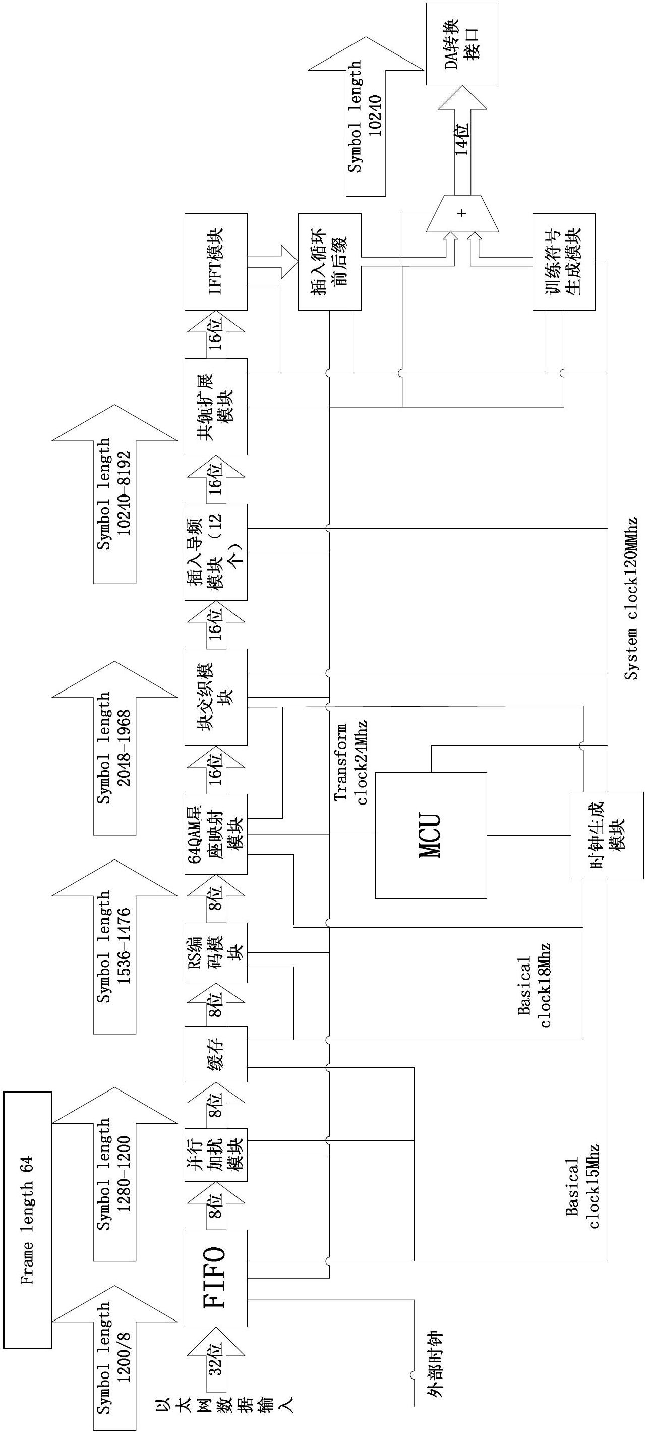
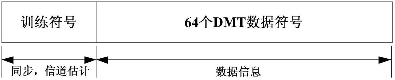
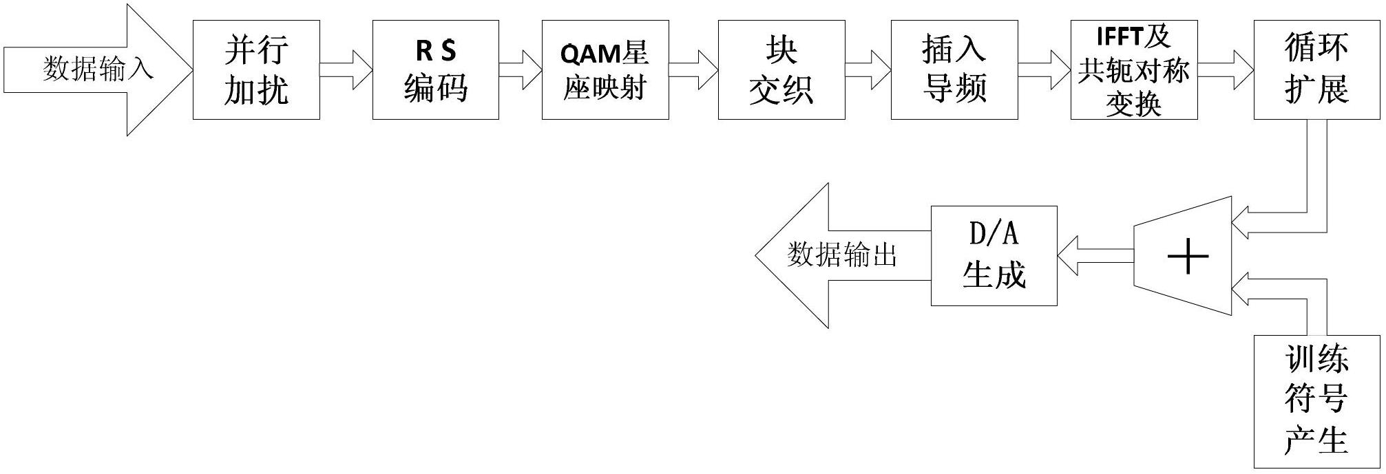
[0063] The cable used in the high-speed 1553B communication bus system developed by the present invention is similar to the twisted pair used in the ADSL (Asymmetric Digital Subscriber Line, hereinafter referred to as ADSL) system, and is 75 ohms. Therefore, DMT modulation technology, which has been maturely applied in ADSL technology, is adopted as the core technology of the high-speed 1553B communication bus system. Using DMT technology, the wideband channel is decomposed into a large number of narrowband sub-channels. The frequency characteristics of each sub-channel are relatively flat, and the data rate that can be transmitted in each sub-channel is low. Using multi-channel parallel transmission technology, the total data rate can be Achieve very high.
[0064] The design starting point of the high-speed 1553B communication bus system is to provide a high-speed data transmission channel for high-speed devices newly connected to the bus while ensuring that the original bus system remains unchanged, thereby forming a new bus system. As known from previous studies, the existing 1553B bus system uses Manchester code for baseband transmission, and the occupied bandwidth is below 20MHz. Therefore, in order to ensure compatibility with the original system and enable high-speed data transmission, this solution uses 4096 sub-carriers. 1370 sub-carriers out of the low frequency, that is, these carriers transmit zero data, and the DMT signal is not transmitted in the low frequency 20MHz bandwidth, which actually occupies a bandwidth of 20M-50M.
[0065] According to the conclusion of previous research and practice, the attenuation of the 1553B bus cable in the 20MHz ~ 50MHz frequency band is less than 14.5dB. Consider in the worst case, the standard noise model in VDSL (Very-high-bit-rate Digital Subscriber loop) is used, that is, it is assumed that there is 140mv additive white Gaussian noise at the receiving end. The characteristics of the bus system, assuming that the transmit power is 2W, the system SNR can be obtained as:
[0066] SNR = 10 * lg P send P noise - 14.4 = 22.8 dB
[0067] Where P send Represents the signal transmission power, P noise Represents the channel noise power, and SNR represents the system signal-to-noise ratio.
[0068] Using Shannon’s formula to calculate the theoretical maximum capacity of the system, the actual bandwidth of the system is about B=28.8MHz:
[0069] C=B*Log 2 (1+SNR)≈351.12Mbps
[0070] Wherein, B indicates that the actual bandwidth unit of the present invention is Hertz (Hz), and C indicates that the channel capacity unit is bits per second (bps).
[0071] The main function of the present invention is to modulate the input data into DMT symbols, including data parallel scrambling, RS coding, QAM constellation mapping, block interleaving, IFFT modulation and other parts; in addition, the sending end must complete the processing of sending data according to a specific frame format. Work includes inserting pilot frequencies, inserting cyclic prefixes and suffixes, and adding training symbols. The FPGA design block diagram is as figure 1 Shown.
[0072] The system has a total of 4096 sub-carriers and uses 64QAM constellation mapping. The number of inserted pilots is 11, and there are a total of 2048 cyclic prefixes and suffixes. According to the characteristics of DMT modulation, the data is conjugated and symmetrically transformed, and the cyclic prefixes and suffixes are added to each output DMT. The symbol length is 10240*14bit. According to the reverse deduction of these parameters, the system has a total of 4096 sub-carriers (including real and virtual carriers) before the conjugate symmetric transformation. After removing the virtual carriers and 11 pilot real carriers, there are a total of 1968 real carriers. Since 64-point QAM constellation mapping is used, and the data bit width after RS ​​encoding is 8bit, the length of the DMT symbol before QAM mapping should be: 1968*6/8=1476; we use (246,200) RS coding, these 1476 data are 6 RS code groups, so the number of DMT symbols before RS coding is 6*200=1200, and in order to increase the data transmission rate and simplify the system design complexity, the input data bit width is selected If it is 8bit, it can be determined that the minimum transmission unit of the high-speed bus system during data transmission should be a DMT symbol packet, that is, the length is 1200*8bit. At the same time, in order to be effectively compatible with the terminal equipment of the high-speed bus system at different transmission speeds, the transmitting end has designed a FIFO (First Input First Output, hereinafter referred to as FIFO) structure to complete the data buffering of the external device and the transmitting end, and in view of the FPGA on-chip The resources are limited, and the FIFO buffer depth cannot be too large. Therefore, the design determines that the system sends a length of 64 DMT symbols per frame while avoiding data loss. Therefore, due to the continuous increase in the length of the DMT symbol during the signal processing, if the system only uses one processing clock, the data will be time-aligned and interrupted due to insufficient processing time. In order to ensure the continuity of the final output data frame at the transmitting end and prevent data loss, this paper designs a multi-clock solution + buffering method to solve this problem, that is, by increasing the subsequent processing speed, it can compensate for the intra-symbol and inter-symbol growth caused by DMT symbol growth. The discontinuity problem. Because multiple clocks tend to cause the setup time and hold time of data to cross clocks to fail to meet the requirements, resulting in metastable state, a cache module is added to each cross-clock domain module to reduce the probability of metastable state generation and improve system reliability Sex.
[0073] The working process of the sender is: after power-on reset, the MCU module (see figure 1 ) Initialize each module and wait for the arrival of valid data. When the external device needs to send data through the high-speed bus, the MCU will activate the training symbol generation module after a certain clock delay after receiving the sending time signal, and generate a training symbol of DMT symbol length as the start of a frame. The external device transmits the data to the FIFO of the sending end according to a certain timing. After the FIFO receives the data, it will notify the parallel scrambler module to accept the data through a handshake signal, and then the parallel scrambler module reads the data in the FIFO according to one DMT symbol at a time, and every two DMT symbols are separated by 80 clock cycles. Then sent to the cache module. The buffer module notifies the RS encoding module after receiving the data. The RS encoding module reads and encodes the data in the buffer module at a time sequence of 46 intervals between every two RS code groups one RS encoding code group (200) at a time. The operation can ensure that the encoded DMT symbols are continuous, and the RS reads every two DMT symbols with an interval of 60 clock cycles. After RS ​​encoding, the data is transmitted to the constellation mapping module for 64QAM mapping, and it is necessary to ensure that the processing interval of every two DMT symbols is 80 clock cycles. Subsequently, block interleaving, pilot insertion, conjugate symmetric transformation and IFFT modulation are performed. After cyclic expansion, multiple consecutive DMT symbols are added to the training symbols and then output to the passing D/A.
[0074] The signal frame of the physical layer of the high-speed 1553B communication bus system is mainly composed of three parts: training symbol area, signal area and data area. The system adopts burst mode transmission, and each burst transmits a complete frame, including training symbols, signal fields and a variable number of DMT data symbols. Among them, the training symbol is mainly used for the receiving end to complete the system synchronization, channel estimation and other functions; behind the training symbol is the signal area, which contains the necessary information required to demodulate the data of this frame. The signal field at this stage should at least contain the following information: Communication process identification, frame sequence number, total number of frames, number of DMT symbols, number of interleaving blocks, QAM format, number of empty packets, number of empty bytes, etc. This field is modulated with reliable BPSK; the last is the data area. The general control module of the physical layer sending end of the high-speed 1553B communication bus system encapsulates these three parts according to a specific timing. figure 2 Shown is the frame structure of the physical layer.
[0075] In order to make the system reach the maximum transmission speed of 100Mbps, considering the bandwidth occupied by the original system, this system uses 4096 sub-carriers for data transmission, including real carriers and virtual carriers. The virtual carrier is not used for data transmission, and zero is added during modulation. In order to be compatible with the original 1553B bus system, the low-frequency 1390 virtual carriers are used to free up the low-frequency 20M bandwidth. In addition, there are 11 real subcarriers used to transmit pilot symbols 1+j. The key parameters of the system are shown in Table 1.
[0076] Table 1 Key system parameters
[0077]
[0078]
[0079] The physical layer sending end of the high-speed 1553B communication bus is actually designed and implemented as a control circuit that can provide high-speed transmission of large data for the high-speed devices in the original 1553B bus system. The control circuit is mainly responsible for sending the data frame of the high-speed device to the destination terminal device in the bus network or receiving data from other terminal devices and then transmitting it to the high-speed device. It only participates in data transmission and sending, and does not analyze related protocols. As the key to the design and realization of the bus interface block, the present invention provides the design and realization model of the physical layer transmitting end, such as image 3 Shown.
[0080] The sender mainly includes the following modules:
[0081] Parallel scrambling module. Parallel scrambling has two main functions. One is to disrupt the sequence of data by scrambling to make it random, and prevent excessively long continuous 1 or 0 sequences from affecting the establishment and maintenance of receiver synchronization; the other is data After scrambling, the statistical characteristics of the original data can be changed without adding redundant bits to make it have statistical characteristics similar to white noise, so as to obtain a predictable power spectrum and peak-to-average power ratio. The schematic diagram of the scrambler is as follows Figure 4 Shown. The scrambler is self-synchronizing, so that the scrambling code can occur autonomously, without the need for a specific code synchronized with the scrambling sequence. The invention adopts the scrambling technology commonly used in the optical transmission system-parallel scrambling. Parallel scrambling technology is different from traditional serial scrambling, which only generates a serial pseudo-random code stream and XOR operation with the input bits, but through careful design of a random sequence generator, it can generate multiple pseudo-random code streams in parallel , Perform XOR operations on these parallel pseudo-random code streams and the received multi-bit symbols respectively, and then output the multiple parallel scrambled symbols at the same time. The code stream produced by parallel-serial conversion of the parallel scrambled data processed in this way is the same as the code stream directly serially scrambled, that is, the functions of the two are the same, but the realization method is different.
[0082] The scrambling algorithm is according to the algorithm expressed by the following equation, and the scrambling algorithm is according to the algorithm expressed by the following equation. At the sampling time nt, the output bit of the data x(nt) should satisfy the following equation:
[0083] x(nt)=x(nt-18)+x(nt-23)+m(nt)
[0084] Where m(nt) is the data bit input at the sampling time nt, x(nt) is the data bit output at the sampling time nt, and x(nt-18) is the data bit output at the sampling time nt-18. x(nt-23) is the data bit output at the sampling time nt-23. All algorithms must be modulo-2 addition. At the beginning of each frame, the shift register is initialized with the sequence "10010101000000010000000"; in specific implementation, scramble The module data entry port has a bit width of 8bit. There is a 23bit shift register inside the module as a pseudo-random code generator. The scrambler works according to the 15MHz clock cycle. 8bit data is input in each clock cycle and the data is transferred in parallel to the shifter. Bit register, the shift register shifts 8 times and produces 8-bit output, the 8-bit parallel output of the shift register is used as the output of the parallel scrambling module, and a handshake signal is output to the next module: when the output is valid, handshake The signal is high, otherwise it is low. reference Figure 4.
[0085] RS encoding module. The scrambled data is sent to the RS encoding module. The RS code can correct random errors and has a certain ability to resist burst errors. This scheme uses byte-oriented RS (246, 200), which is a shortened code of RS (255, 209) code. The code length is 246 bytes, including 200 information bytes and 46 check bytes. The maximum correctable error is t=(nk)/2=23 bytes. One of the reasons for choosing this code is that we want each DMT symbol to contain an integer number of code words. When the subcarriers are modulated by 16QAM, 64QAM or 256QAM, the codewords contained in each DMT symbol are 4, 6, and 8, respectively. The performance inflection point of the RS(255,209) code appears around one percent of the bit error rate. That is, if the bit error rate is less than one percent in the case of unencoding, the system bit error rate will be greatly reduced after the code is adopted. At this time, increasing the signal-to-noise ratio will not significantly improve the performance. Otherwise, the code is useless to the system. In the specific implementation, the IP core (Intellectual Property core, or IP core) Reed-Solomon Compiler v10.1 provided by Altera is used. The module works under a clock of 18MHz. The input bit width and output bit width are both 8bit. Every 200 8-bit input codes are 246 8-bit RS code outputs.
[0086] QAM constellation mapping module. Because the high-speed 1553B communication bus system requires high-speed data transmission on a limited spectrum. Therefore, in order to improve the spectrum utilization of the system and enable the system to obtain a higher transmission speed in a narrower frequency band, the present invention selects Quadrature Amplitude Modulation (QAM) as the modulation mode for each sub-channel of the system. In the digital system, the digital signal is mainly subjected to multi-ary quadrature amplitude modulation and mapping. Different modulation orders M can be selected to achieve the transmission rate of the communication system. The present invention mainly adopts 64QAM constellation mapping. After constellation mapping for the unit, it becomes the corresponding complex number. We use 16bit signed numbers to represent this kind of complex numbers, the highest bit is the sign bit, one integer bit, the rest are decimal bits, and the complement is used to represent negative numbers. In order to minimize the excessive noise generated when the constellation points change during the constellation mapping process, and minimize the number of different bits of adjacent constellation points, the gray code is used to encode the constellation points. Input 6bit data b 5 b 4 b 3 b 2 b 1 b 0 Perform constellation mapping, where b 2 b 1 b 0 Corresponding to the imaginary part Q, b of the mapped data 5 b 4 b 3 Corresponding to the real part I of the mapped data, the mapping follows the principle of high-order priority, and the obtained symbol corresponds to a certain constellation point (I, Q), and the output result of the constellation encoder is I+jQ. The constellation point is represented by (I, Q), and I and Q must be located on odd integers ±1, ±3, ±5, etc. The present invention uses Gray code constellation diagrams, adopts three modulation modes of 16QAM, 64QAM and 256QAM, and their constellation diagrams are all square. Figure 5 It is a gray code constellation diagram of 64QAM. Since the training symbols and signal fields designed in this paper are all BPSK modulated, and the subsequent data segments are modulated by multi-ary quadrature amplitude modulation, this will result in uneven transmission signal power, which is not conducive to synchronization and equalization. Therefore, the average power of the constellation should be normalized so that all constellations have the same average power regardless of the size of the constellation. The normalization is based on the BPSK signal power, and the multi-ary quadrature amplitude modulation constellation points are scaled:
[0087] Z i =(X i +jY i )λ
[0088] Among them, λ represents the power normalization factor, X i And Y i Respectively represent the real part and imaginary part of the constellation point before power normalization, Z i Represents the complex number sequence output by the constellation encoder after power normalization, and its value is shown in Table 2. In specific implementation, first convert 8-bit data into 6-bit data, that is, create a 24-bit register, store 8-bit-wide data in the register under the 18MHz clock, and then follow the 24MHz clock when it is full. Read the register with 6bit width, and then repeat the above process to complete the bit width conversion; then, input 6bit data b 5 b 4 b 3 b 2 b 1 b 0 Use branch selection sentences for constellation mapping, where b 2 b 1 b 0 Corresponding to the imaginary part Q, b of the mapped data 5 b 4 b 3 Corresponding to the real part I of the mapped data, the mapping follows the principle of high order first, and the obtained symbol corresponds to a certain constellation point (I, Q), and the mapping result refers to Figure 5 And table 2.
[0089] Table 2 Power normalization factor λ comparison table
[0090]
[0091]
[0092] Block interleaving module. The main function of block interleaving is to disrupt the original data sequence structure according to a certain rule, and the purpose is to separate multiple adjacent data as far as possible. When a long burst error occurs in the data sequence after this processing, the original continuous error sequence can be discretized. If the interleaving depth is large, the discretized burst error can be approximated as a random error. . Since the RS code can only correct relatively short burst errors, in order to enhance the frequency selective fading against burst sums, the present invention uses block interleaving to spread the errors to a large number of RS code words, so that the errors are evenly distributed in each The frequency diversity is thus obtained within the codeword. The principle is: the data to be interleaved at the sender is evenly divided into m code groups with s data segments, m is called the interleaver depth, and s is the interleaver constraint length. The code group can be represented by an s×m matrix , To be interleaved data press [a 11 , A 12 ,...A 1s , A 21 , A 22...a ms ]Sequentially enter the interleaving matrix, and then press [a 11 , A 21 ,...A m1 , A 12 , A 22...a ms ]Sequential output to complete the packet interleaving of data. According to the principle of grouping interleaving, when the interleaved data suffers burst interference in the channel, a continuous error code occurs. After deinterleaving, the continuous error codeword is dispersed into each code group. The interval between two adjacent erroneous codewords is n, and all erroneous codewords can be corrected by using the RS error correction code. Since block interleaving will cause a large delay, the interleaving block should not be too large. In the specific implementation, a temporary memory is established as an interleaver. The interleaver has 246 rows and 8 columns, and each unit stores one byte. The delay caused by interleaving and deinterleaving is 3936 bytes. When interleaving, write in rows and read in columns. The read and write clocks are both 24MHz. When 64QAM is used, each interleaving block is filled with exactly one DMT symbol. Assuming a set of data streams entering the interleaver: r represents a row, c represents a column (colomn), the order in which the data is written into the memory by rows is: r1c1, r1c2,..., r1c7, r1c8, r2c1, r2c2,..., r246c7, r246c8; read from RAM in the order of columns: r1c1, r2c1, r3c1,..., r245c1, r246c1, r1c2, r2c2,... ..., r1c8, r2c8,..., r245c8, r246c8.
[0093] Image 6 with Figure 7 The schematic diagram of the interleaving module is written in rows and read in columns.
[0094] Pilot insertion. In a multi-carrier system, known pilot data is usually transmitted on certain subcarriers so that the receiver can use the known pilot data to perform operations such as channel estimation and phase tracking. This text transmits data 1+j according to the 11 pilot subcarrier positions listed in Table 1 in each DMT symbol to complete frequency offset estimation at the receiving end. In the specific implementation, a 13-bit counter is set to count the sequence number of the current frequency point, and the data at the corresponding frequency point is allocated using the branch selection statement. When the current frequency point counting result is a virtual carrier, 0 is transmitted, and the current frequency point When the point counting result is the real carrier, the corresponding actual data is transmitted. When the current frequency point counting result is the pilot, the data 1+j is transmitted. Table 1 lists the positions of the real carrier, virtual carrier and pilot. Figure 8 It also indicates the locations of virtual carriers, real carriers, and pilots.
[0095] The IFFT module and the conjugate symmetric transformation module use IDFT to modulate the output of the constellation encoder to the DMT subcarrier. It transforms the N complex values ​​generated by the constellation encoder to represent the frequency domain into 2N real values ​​representing the time domain . The real-valued sequence is a time-domain sampling of a DMT symbol, and it just satisfies the Nyquist sampling theorem. Considering that the output of the constellation encoder is complex, in order to obtain 2N real numbers through IFFT, the complex number sequence output by the constellation encoder should be conjugate extended to make the input sequence have conjugate symmetry:
[0096] S i =Z i , I=0, 1,..., N-1
[0097] S i =conj(Z 2N-i ), i=N+1, N+2,..., 2N-1
[0098] Where Z i Represents the complex number sequence output by the constellation encoder, S i Means to Z i The complex number sequence obtained by conjugate extension, conj() represents the conjugate complex number, N represents the number of the complex sequence generated by the constellation encoder, i represents the subscript of the complex sequence obtained by the conjugate extension, and the value range is (i = 0, 1,..., 2N-1).
[0099] Then to S i Implement 2N-point IFFT:
[0100] x n = X i = 0 2 N - 1 exp ( j · 2 · π n · i 2 · N ) · S i
[0101] Where x n Represents 2N real numbers representing time domain obtained by inverse fast Fourier transform, n represents x n The subscript of, the value range is (n=0,1,...,2N-1), exp() means finding the natural exponent, and other symbols have the same meaning as the above formula.
[0102] According to the parameters of the present invention, the QAM symbols are modulated on 1968 real carriers, and the remaining carriers are filled with zeros. After IFFT transformation, 8192 real-valued sampling points of the modulated waveform are obtained. These sampling points are passed through D/A (ie, digital to analog converter, Hereinafter referred to as D/A) conversion, filtering and amplifying operations can be injected into the channel for transmission. In the specific implementation, the conjugate expansion is performed first and then the IFFT transformation is performed. First, build a 13-bit counter to count the frequency point number. When the count result of the counter is 1 to 4096, the output result is the same as the input result. When the count result of the counter is 4097 to 8192, it means that it is in conjugate extension. In the part, the result of the conjugate transformation is assigned to the output according to the conjugate symmetry formula. At this time, the data bit width is 16bit; the IFFT part uses the IP core (Intellectual Property core or IP core) FFT MegaCore Function v10 provided by Altera. 1. The module works under a 120MHz clock. After configuring the input bit width and output bit width to be 16bit and works in block floating point and inverse transform mode, the IP core can be used to achieve very efficient IFFT.
[0103] Cycle expansion module. Unlike OFDM, which is mainly used in wireless communications, DMT is mainly used in wired communications environments. Due to the absence of factors such as the delay spread of the wireless channel and carrier frequency offset, inter-symbol crosstalk has become the main factor affecting the performance of the DMT system. In order to minimize the inter-code crosstalk, the cyclic extension adopted by the present invention not only includes adding a cyclic prefix, but also needs to add a cyclic suffix. Suppose the channel impulse response is h(t), which is the convolution of the filter, amplifier and channel at both ends of the transceiver. The period of response from the generation of the response to the peak value is called "delay", and the period of response from the peak to the disappearance of the response is called "tailing". Time delay will cause front crosstalk, and tailing will cause rear crosstalk. Theoretically, the length of the cyclic prefix should be equal to the trailing length, and the length of the cyclic suffix should be equal to the time extension, so that the inter-symbol crosstalk can be completely eliminated. If the time delay is small, that is, h(t) reaches the peak quickly, the cyclic suffix may not be added. IDFT output x n The last L cp Samples added to 2N output IDFT samples x n Above, as a cyclic prefix (CP). x n The beginning of the L cs Samples added to x n +L cp On the sample block, it is used as a cyclic suffix (CS). The length of the cyclic extension (CE) part is L CE =L CP +L CS. Such as Image 6 Shown. During specific implementation, a buffer of 8192*16 bits is established, and the results of the IFFT transform are buffered in order. Next, set up a 14-bit counter. When the count result of the counter is 1~1920, read the data from the registers 6273~8192 as the cyclic prefix in order. When the count result of the counter is 1921~10112, read the registers 1~in order. 8192 data, when the count result of the counter is 10113~10240, read the data of buffer 1~128 in order as the cyclic suffix.
[0104] Training symbol generation module. This article inserts a DMT symbol size training symbol at the beginning of each data frame (including multiple DMT symbols) so that the receiver can use this known training symbol for frame synchronization and symbol synchronization operations, and it is also used for channel estimation and Frequency domain equalization. The training symbols are obtained by BPSK modulation from the m sequence, and the zeros in the m sequence should be replaced with -1. The selected tap coefficient of the m sequence is [1 1 0 1 0 1 0 1 0 1 1 0]. In specific implementation, since the training symbols are known, the production of training symbols is realized by reading ROM, that is, a DMT symbol is obtained after the known training symbol sequence is calculated by the matlab simulation model of the transmitting end of the high-speed 1553B communication bus system. After fixed-point quantization, it is stored in the FPGA on-chip ROM. When needed, the read address generator generates the read address of the ROM. Since the training symbol also needs to be cyclically extended, the address of the cyclic extension sequence is generated first, and then the DMT symbol address is sequentially generated After the two are combined, the generation of training symbols is completed.
[0105] Selection of key system parameters: In order to enable the system to achieve a maximum transmission speed of 100Mbps, considering the bandwidth occupied by the original system, this system uses 4096 sub-carriers for data transmission, including real carriers and virtual carriers. The virtual carrier is not used for data transmission, and zero is added during modulation. The serial numbers of the virtual carriers are 0~1389 and 3369~4095. In order to be compatible with the original 1553B bus system, the low frequency 1390 virtual carriers are used to free up the low frequency 20M bandwidth, and the high frequency virtual carriers are used to increase the sampling rate. In addition, there are 11 real subcarriers used to transmit pilot symbols 1+j. See Table 1 for detailed parameters. RS code selection (246, 200), it is a shortened code of (255, 209), one of the reasons for choosing this code is because we hope that each DMT symbol contains an integer number of code words, when the sub-carrier adopts 16QAM, 64QAM or At 256QAM, the codewords contained in each DMT symbol are 4, 6, and 8, respectively. Due to the delay caused by interleaving, the selection of the interleaving depth is a trade-off process. The interleaver set in the present invention is 246 columns and 8 rows. When 64QAM is used, each interleaving block is filled with exactly one DMT symbol.

PUM

no PUM

Description & Claims & Application Information

We can also present the details of the Description, Claims and Application information to help users get a comprehensive understanding of the technical details of the patent, such as background art, summary of invention, brief description of drawings, description of embodiments, and other original content. On the other hand, users can also determine the specific scope of protection of the technology through the list of claims; as well as understand the changes in the life cycle of the technology with the presentation of the patent timeline. Login to view more.
Why Eureka
Try Eureka