Method and device for mapping gain conversion of image sensors

An image sensor and mapping method technology, which is applied in the field of image sensors, can solve the problems of gain monotonicity, poor precision, and complex gain calculation, and achieve the effect of simplifying the gain conversion process, avoiding non-monotonic changes, and reducing gain errors

Active Publication Date: 2012-09-26
深圳市夜行人科技有限公司
View PDF7 Cites 4 Cited by
  • Summary
  • Abstract
  • Description
  • Claims
  • Application Information

AI Technical Summary

Problems solved by technology

Among them, the first-stage amplifying circuit is a variable gain amplifier (Programmable Gain Amplifier, PGA), and the corresponding gain is called PGA gain. Its advantage is that it can provide a relatively large gain, but the accuracy is relatively poor, and the error may also be relatively large.
The second-stage amplification circuit is an analog-to-digital converter (Analog to Digital Converter, ADC). The amplification function can also be achieved by adjusting the full-scale voltage of the ADC. The corresponding gain is called the ADC gain. Its advantage is that it has higher precision, but The gain that can be provided is relatively small, and the calculation of the gain is more complicated
[0008] It should be noted that the monotonicity of the gain must be guaranteed during the gain mapping process, that is, the greater the value transmitted by the AGC circuit, the greater the product of the three-stage gain must be, otherwise the AGC circuit will not work properly. The output image is likely to appear flickering
However, due to process deviations in the manufacture of integrated circuits, the actual and theoretical values ​​of PGA gain and ADC gain will have certain errors
The process deviation easily affects the gain mapping process, and the monotonicity of the gain in the gain mapping process cannot be guaranteed, thereby reducing the stability of the image brightness
[0009] A Chinese patent with the notification number CN1910903B discloses an image sensor with an amplifying circuit, but the above-mentioned problems cannot be solved in said Chinese patent

Method used


Image

  • Method and device for mapping gain conversion of image sensors
  • Method and device for mapping gain conversion of image sensors
  • Method and device for mapping gain conversion of image sensors

Examples


Embodiment Construction

[0037] In order to make the above objects, features and advantages of the present invention more comprehensible, specific implementations of the present invention will be described in detail below in conjunction with the accompanying drawings.

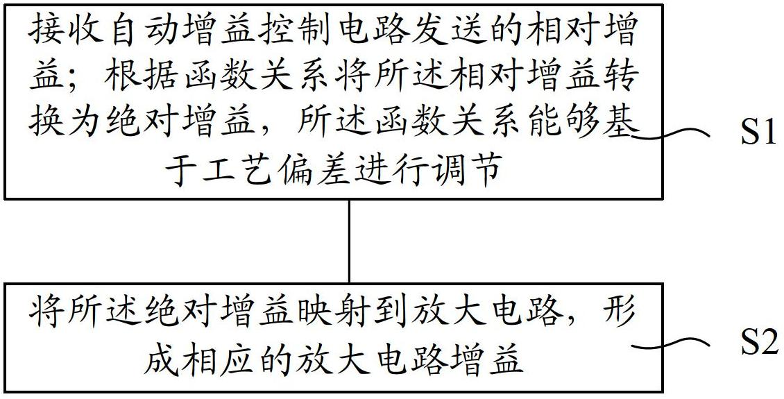
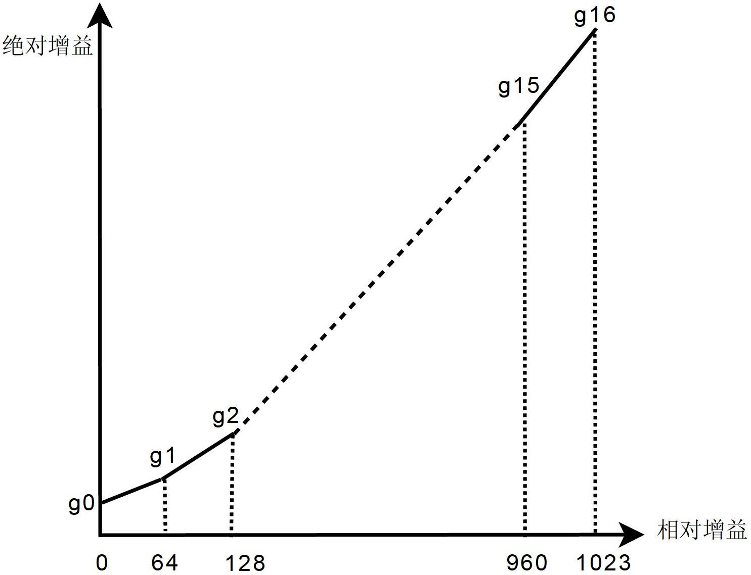
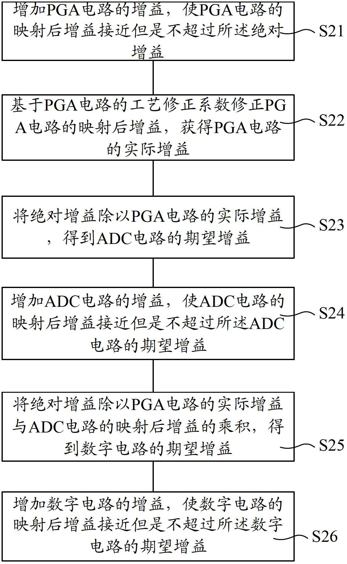
[0038] In order to solve the problems in the prior art, the present invention provides a gain conversion mapping method of an image sensor. refer to figure 1 , shows a schematic flowchart of an embodiment of a method for gain conversion mapping of an image sensor according to the present invention.

[0039] Generally, an image sensor includes pixels arranged in a matrix and circuit units connected to the pixels. Wherein, the pixel is used to convert the received light signal into an output voltage; the circuit unit is used to adjust and process the output voltage, and output an image based on the output voltage.

[0040] The circuit unit includes an amplifier circuit and an automatic gain control circuit (Automatic Gain Control, AGC)...


PUM


Abstract

The invention discloses a method and a device for mapping gain conversion of image sensors. The image sensors comprise automatic gain control circuits and amplification circuits. The method includes the steps: receiving relative gain transmitted by the automatic gain control circuit; converting the relative gain into absolute gain according to a function relationship which is adjustable based on process variation; and mapping the absolute gain to each amplification circuit so as to form corresponding amplification circuit gain. The device comprises a gain conversion circuit and a gain mapping circuit, wherein the gain conversion circuit is connected with each automatic gain control circuit and used for receiving the relative gain transmitted by each automatic gain control circuit and converting the relative gain into the absolute gain according to the function relationship which is adjustable based on process variation; and the gain mapping circuit is connected with the gain conversion circuit and used for mapping the absolute gain to gain of each amplification circuit. By the method and the device, errors during gain conversion mapping caused by the process variation are decreased.

Description

technical field [0001] The present invention relates to the field of image sensors, in particular to a gain conversion mapping method and device for an image sensor. Background technique [0002] Image sensors belong to the optoelectronic components in the optoelectronic industry. With the rapid development of digital technology, semiconductor manufacturing technology and the Internet, the market and the industry are now facing the arrival of the era of video, video, and communication integration across various platforms. The beauty of the daily life of future human beings. Therefore, image sensor-related products have become the focus of the industry at present and in the future, attracting investment from many manufacturers. [0003] Taking a CMOS image sensor (complementary metal oxide image sensor) as an example, the CMOS image sensor includes a plurality of pixels arranged in a matrix and circuit units connected to the plurality of pixels. Wherein, the pixel is used f...

Claims


Application Information

Patent Timeline
Patent Type & Authority Applications(China)
IPC IPC(8): H04N5/3745H04N5/335
Inventor 池国泉
Owner 深圳市夜行人科技有限公司
Why Eureka
Try Eureka