Light-emitting diode display back plate, manufacturing method and display device for light-emitting diode display back plate

A technology of light-emitting diodes and display backplanes, applied in the field of display devices, light-emitting diode display backplanes and manufacturing methods thereof, can solve problems such as unfavorable large-scale production, increased equipment investment, and increased manufacturing costs of light-emitting diode display backplanes. Effects that improve the glow quality

Active Publication Date: 2014-08-27
BOE TECH GRP CO LTD
View PDF6 Cites 2 Cited by
  • Summary
  • Abstract
  • Description
  • Claims
  • Application Information

AI Technical Summary

Problems solved by technology

Mainly utilize 60% CF at present 4 In the environment of CVD (Chemical Vapor Deposition, chemical vapor deposition), the surface of the PDL layer is fluorinated to improve the wetting characteristics of the surface of the PDL layer, but this method needs to increase the investment of equipment and increase the cost of the LED display backplane. Manufacturing cost, not conducive to mass production

Method used


Image

  • Light-emitting diode display back plate, manufacturing method and display device for light-emitting diode display back plate
  • Light-emitting diode display back plate, manufacturing method and display device for light-emitting diode display back plate
  • Light-emitting diode display back plate, manufacturing method and display device for light-emitting diode display back plate

Examples


Embodiment Construction

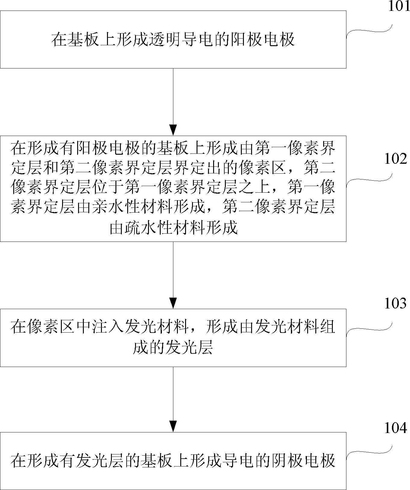
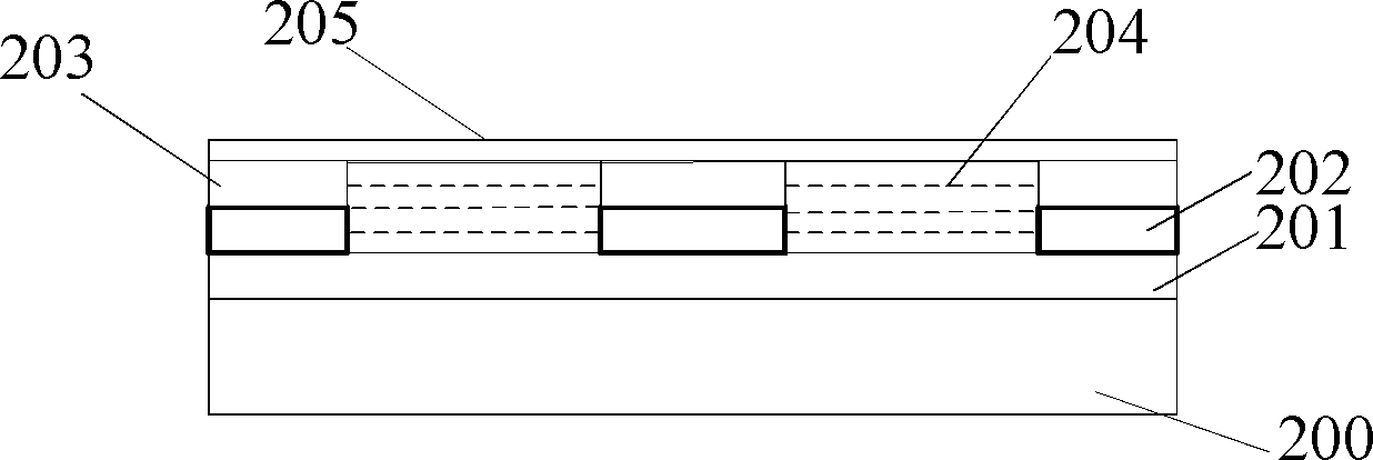
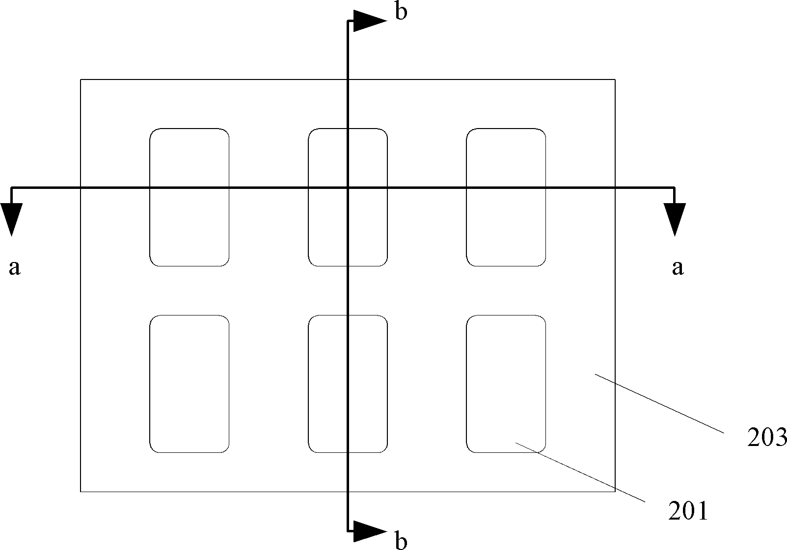
[0038] In order to make the technical problems, technical solutions and advantages to be solved by the embodiments of the present invention clearer, the following will describe in detail with reference to the drawings and specific embodiments.

[0039] The embodiments of the present invention aim at fluorinating the surface of the PDL layer in the prior art in order to ensure that the printed droplets smoothly and evenly cover the pixel area defined by the pixel defining layer and prevent the droplets from flowing to adjacent pixel areas. treatment, thereby improving the wetting characteristics of the surface of the PDL layer, but this method needs to increase the investment in equipment, increases the manufacturing cost of the light-emitting diode display backplane, and is not conducive to the problem of mass production. A light-emitting diode display backplane and its The manufacturing method and the display device enable the luminescent material to be flatly spread on the LE...


PUM

PropertyMeasurementUnit
thicknessaaaaaaaaaa
thicknessaaaaaaaaaa

Abstract

The invention provides a light-emitting diode display backplane, a manufacturing method thereof, and a display device, which belong to the display field. The manufacturing method of the light-emitting diode display backplane includes: forming a transparent and conductive anode electrode on a substrate; forming a pixel region defined by a first pixel defining layer and a second pixel defining layer on the substrate formed with the anode electrode, The second pixel defining layer is located on the first pixel defining layer, the first pixel defining layer is formed of a hydrophilic material, and the second pixel defining layer is formed of a hydrophobic material; in the pixel area Injecting a luminescent material into the luminescent material to form a luminescent layer composed of the luminescent material; forming a conductive cathode electrode on the substrate on which the luminescent layer is formed. The technical scheme of the present invention enables the luminous material to be flatly spread on the backplane of the light-emitting diode display, thereby improving the luminous quality of the backplane of the light-emitting diode display.

Description

technical field [0001] The invention relates to the field of display, in particular to a light-emitting diode display backplane, a manufacturing method thereof, and a display device. Background technique [0002] OLED (Organic Light-Emitting Diode, organic light-emitting diode) / PLED (polymer light-emitting diode, polymer light-emitting diode) display backplane is composed of glass substrate, ITO (indium tin oxide, indium tin oxide) anode (Anode), organic Emitting Material Layer (Emitting Material Layer) and Cathode (Cathode), etc., where the thin and transparent ITO anode and metal cathode sandwich the organic light-emitting layer like a sandwich, when the voltage injected into the anode hole (Hole) and When the electrons from the cathode are combined in the organic light emitting layer, the organic material in the organic light emitting layer is excited to emit light. [0003] At present, when preparing a light-emitting diode display backplane, a photoresist is coated on a...

Claims


Application Information

Patent Timeline
Patent Type & Authority Patents(China)
IPC IPC(8): H01L27/32F21Y101/02
CPCH01L27/3283H01L27/3246H01L51/5012H01L27/153H01L51/0005H01L51/56H10K59/122H10K59/173H10K71/135H10K50/11H10K71/40H10K71/00
Inventor 姜春生
Owner BOE TECH GRP CO LTD
Why Eureka
Try Eureka